SLOS545D November 2008 – December 2014 TLV320AIC3107
UNLESS OTHERWISE NOTED, this document contains PRODUCTION DATA.
- 1 Features
- 2 Applications
- 3 Description
- 4 Simplified Block Diagram
- 5 Revision History
- 6 Description (Continued)
- 7 Pin Configuration and Functions
- 8 Specifications
- 9 Parameter Measurement Information
-
10Detailed Description
- 10.1 Overview
- 10.2 Functional Block Diagram
- 10.3
Feature Description
- 10.3.1 Hardware Reset
- 10.3.2 Digital Audio Data Serial Interface
- 10.3.3 Audio Data Converters
- 10.3.4 Audio Analog Inputs
- 10.3.5 Analog Line Output Drivers
- 10.3.6 Analog High Power Output Drivers
- 10.3.7 Input Impedance and VCM Control
- 10.3.8 General Purpose I/O
- 10.3.9 MICBIAS Generation
- 10.3.10 Class-D Speaker Driver
- 10.3.11 Short Circuit Output Protection
- 10.3.12 Jack and Headset Detection
- 10.4 Device Functional Modes
- 10.5 Programming
- 10.6 Register Maps
- 11Application and Implementation
- 12Power Supply Recommendations
- 13Layout
- 14Device and Documentation Support
- 15Mechanical, Packaging, and Orderable Information
Package Options
Mechanical Data (Package|Pins)
Thermal pad, mechanical data (Package|Pins)
- RSB|40
Orderable Information
1 Features
- Stereo CODEC With Integrated Mono Class-D Amplifier
- High Performance Audio DAC
- 97-dBA Signal-to-Noise Ratio (Single Ended)
- 16/20/24/32-Bit Data
- Supports Sample Rates From 8 kHz to 96 kHz
- 3D/Bass/Treble/EQ/De-Emphasis Effects
- Flexible Power Saving Modes and Performance are Available
- High Performance Audio ADC
- 92-dBA Signal-to-Noise Ratio
- Supports Rates From 8 kHz to 96 kHz
- Digital Signal Processing and Noise Filtering Available During Record
- Seven Audio Input Pins
- Programmable as 6 Single-Ended or 3 Fully Differential Inputs
- Capability for Floating Input Configurations
- Multiple Audio Output Drivers
- Mono Fully Differential or Stereo Single-Ended Headphone Drivers
- Single-Ended Stereo Line Outputs
- Mono 1 W Class-D BTL 8Ω Speaker Driver
- Low Power Consumption: 15-mW Stereo 48-kHz Playback With 3.3-V Analog Supply
- Ultra-Low Power Mode with Passive Analog Bypass
- Programmable Input/Output Analog Gains
- Automatic Gain Control (AGC) for Record
- Programmable Microphone Bias Level
- Programmable PLL for Flexible Clock Generation
- I2C™ Control Bus
- Audio Serial Data Bus Supports I2S, Left/Right-Justified, DSP, and TDM Modes
- Extensive Modular Power Control
- Power Supplies:
- Speaker Amp: 2.7 V – 5.5 V
- Analog: 2.7 V – 3.6 V.
- Digital Core: 1.525 V – 1.95 V
- Digital I/O: 1.1 V – 3.6 V
- Packages: 5-mm × 5-mm 40-QFN, 0.4-mm Pitch
3.563-mm × 3.376-mm 42-DSBGA, 0.5 mm Pitch
(Product Preview)
2 Applications
- Cellular Handsets
- Digital Cameras
- Portable Media Players
- General Portable Audio Equipment
3 Description
The TLV320AIC3107 is a low power stereo audio codec with stereo headphone amplifier, and mono class-D speaker driver, as well as multiple inputs and outputs programmable in single-ended or
fully differential configurations.
Device Information(1)
| PART NUMBER | PACKAGE | BODY SIZE (MAX) |
|---|---|---|
| TLV320AIC3107 | WQFN (40) | 5.15 mm × 5.15 mm |
| DSBGA (42) | 3.563 mm × 3.376 mm |
- For all available packages, see the orderable addendum at the end of the datasheet.
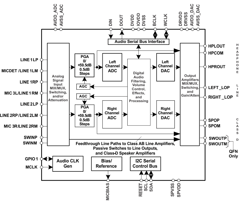
4 Simplified Block Diagram