SLOS545D November   2008  – December 2014 TLV320AIC3107

UNLESS OTHERWISE NOTED, this document contains PRODUCTION DATA.  

  1. Features
  2. Applications
  3. Description
  4. Simplified Block Diagram
  5. Revision History
  6. Description (Continued)
  7. Pin Configuration and Functions
  8. Specifications
    1. 8.1 Absolute Maximum Ratings
    2. 8.2 ESD Ratings
    3. 8.3 Recommended Operating Conditions
    4. 8.4 Thermal Information
    5. 8.5 Dissipation Ratings
    6. 8.6 Electrical Characteristics
    7. 8.7 Audio Data Serial Interface Timing Requirements
    8. 8.8 Typical Characteristics
  9. Parameter Measurement Information
  10. 10Detailed Description
    1. 10.1 Overview
    2. 10.2 Functional Block Diagram
    3. 10.3 Feature Description
      1. 10.3.1  Hardware Reset
      2. 10.3.2  Digital Audio Data Serial Interface
        1. 10.3.2.1 Right Justified Mode
        2. 10.3.2.2 Left Justified Mode
        3. 10.3.2.3 I2S Mode
        4. 10.3.2.4 DSP Mode
        5. 10.3.2.5 TDM Data Transfer
      3. 10.3.3  Audio Data Converters
        1. 10.3.3.1 Audio Clock Generation
        2. 10.3.3.2 Stereo Audio ADC
          1. 10.3.3.2.1 Stereo Audio ADC High Pass Filter
          2. 10.3.3.2.2 Automatic Gain Control (AGC)
            1. 10.3.3.2.2.1 Target Level
            2. 10.3.3.2.2.2 Attack Time
            3. 10.3.3.2.2.3 Decay Time
            4. 10.3.3.2.2.4 Noise Gate Threshold
            5. 10.3.3.2.2.5 Maximum PGA Gain Applicable
        3. 10.3.3.3 Stereo Audio DAC
          1. 10.3.3.3.1 Digital Audio Processing for Playback
          2. 10.3.3.3.2 Digital Interpolation Filter
          3. 10.3.3.3.3 Delta-Sigma Audio DAC
          4. 10.3.3.3.4 Audio DAC Digital Volume Control
          5. 10.3.3.3.5 Increasing DAC Dynamic Range
          6. 10.3.3.3.6 Analog Output Common-Mode Adjustment
          7. 10.3.3.3.7 Audio DAC Power Control
      4. 10.3.4  Audio Analog Inputs
      5. 10.3.5  Analog Line Output Drivers
      6. 10.3.6  Analog High Power Output Drivers
      7. 10.3.7  Input Impedance and VCM Control
      8. 10.3.8  General Purpose I/O
      9. 10.3.9  MICBIAS Generation
      10. 10.3.10 Class-D Speaker Driver
      11. 10.3.11 Short Circuit Output Protection
      12. 10.3.12 Jack and Headset Detection
    4. 10.4 Device Functional Modes
      1. 10.4.1 Bypass Path Mode
        1. 10.4.1.1 Analog Input Bypass Path Functionality
        2. 10.4.1.2 ADC PGA Signal Bypass Path Functionality
        3. 10.4.1.3 Passive Analog Bypass During Powerdown
      2. 10.4.2 Digital Audio Processing For Record Path
    5. 10.5 Programming
      1. 10.5.1 I2C Control Mode
        1. 10.5.1.1 I2C Bus Debug in a Glitched System
        2. 10.5.1.2 Register Map Structure
    6. 10.6 Register Maps
      1. 10.6.1 Control Registers
      2. 10.6.2 Output Stage Volume Controls
        1. 10.6.2.1 Page 1 / Register 10:   Left Channel Audio Effects Filter N4 Coefficient LSB Register
  11. 11Application and Implementation
    1. 11.1 Application Information
    2. 11.2 Typical Application
      1. 11.2.1 Design Requirements
      2. 11.2.2 Detailed Design Procedure
      3. 11.2.3 Application Curves
  12. 12Power Supply Recommendations
  13. 13Layout
    1. 13.1 Layout Guidelines
    2. 13.2 Layout Example
  14. 14Device and Documentation Support
    1. 14.1 Trademarks
    2. 14.2 Electrostatic Discharge Caution
    3. 14.3 Glossary
  15. 15Mechanical, Packaging, and Orderable Information

Package Options

Mechanical Data (Package|Pins)
Thermal pad, mechanical data (Package|Pins)
Orderable Information

13 Layout

13.1 Layout Guidelines

PCB design is made considering the application, and the review is specific for each system requirements. However, general considerations can optimize the system performance.

  • The TLV320AIC3107IRSB thermal pad should be connected to analog output driver ground using multiple VIAS to minimize impedance between the device and ground.
  • SPVSS balls of TLV320AIC3107IYZF are recommended to be soldered directly to Class-D ground.
  • SPVSS balls of TLV320AIC3107IYZF are recommended to be soldered directly to Class-D ground.
  • The TLV320AIC3107 requires the decoupling capacitors to be placed as close as possible to the device power supply terminals.
  • If possible, route the differential audio signals differentially on the PCB. This is recommended to get better noise immunity.

13.2 Layout Example

AIC3107_QFP_LayoutExample.png
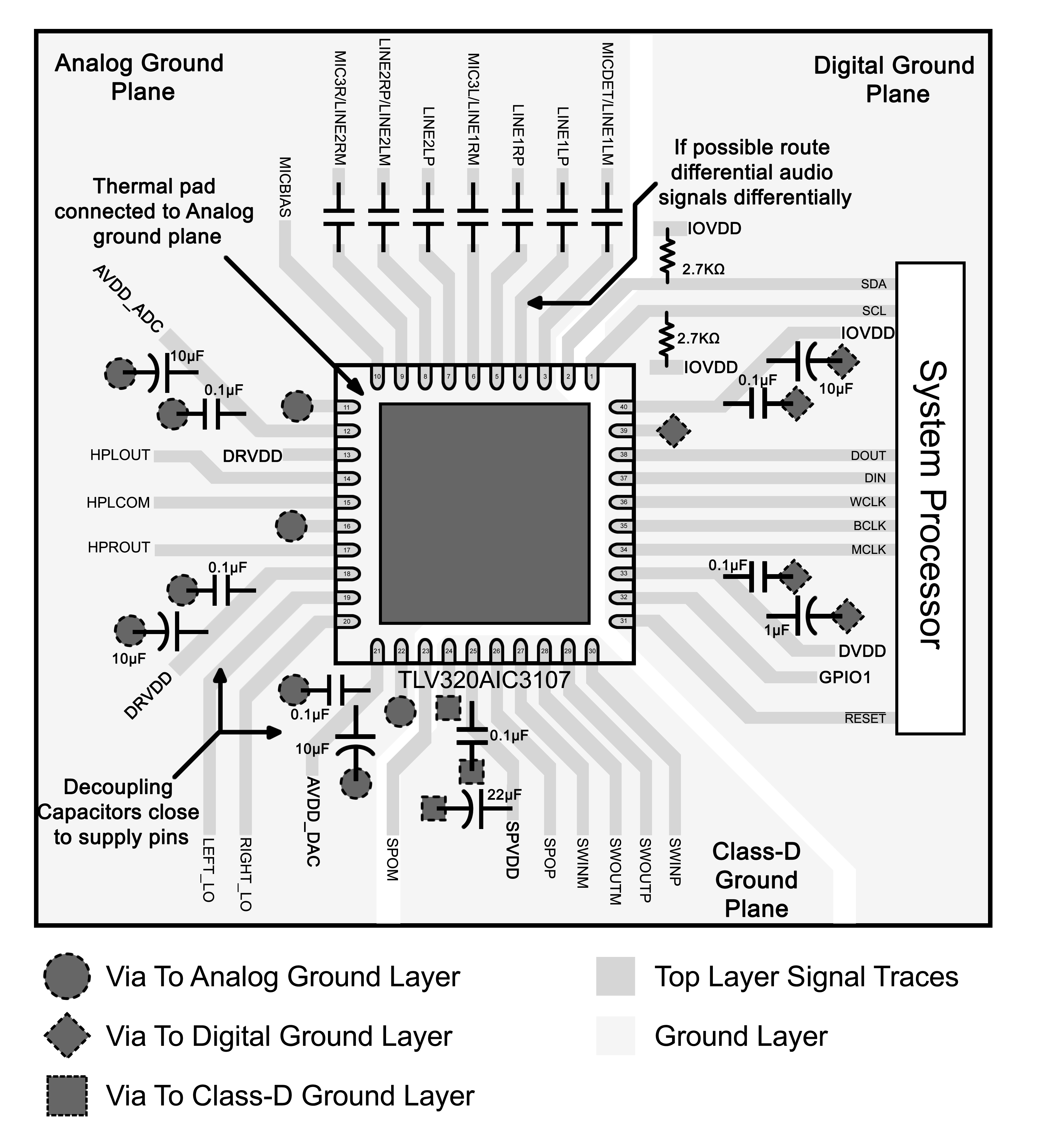
Figure 41. AIC3107 WQFN Layout Example
AIC3107_BGA_LayoutExample.png
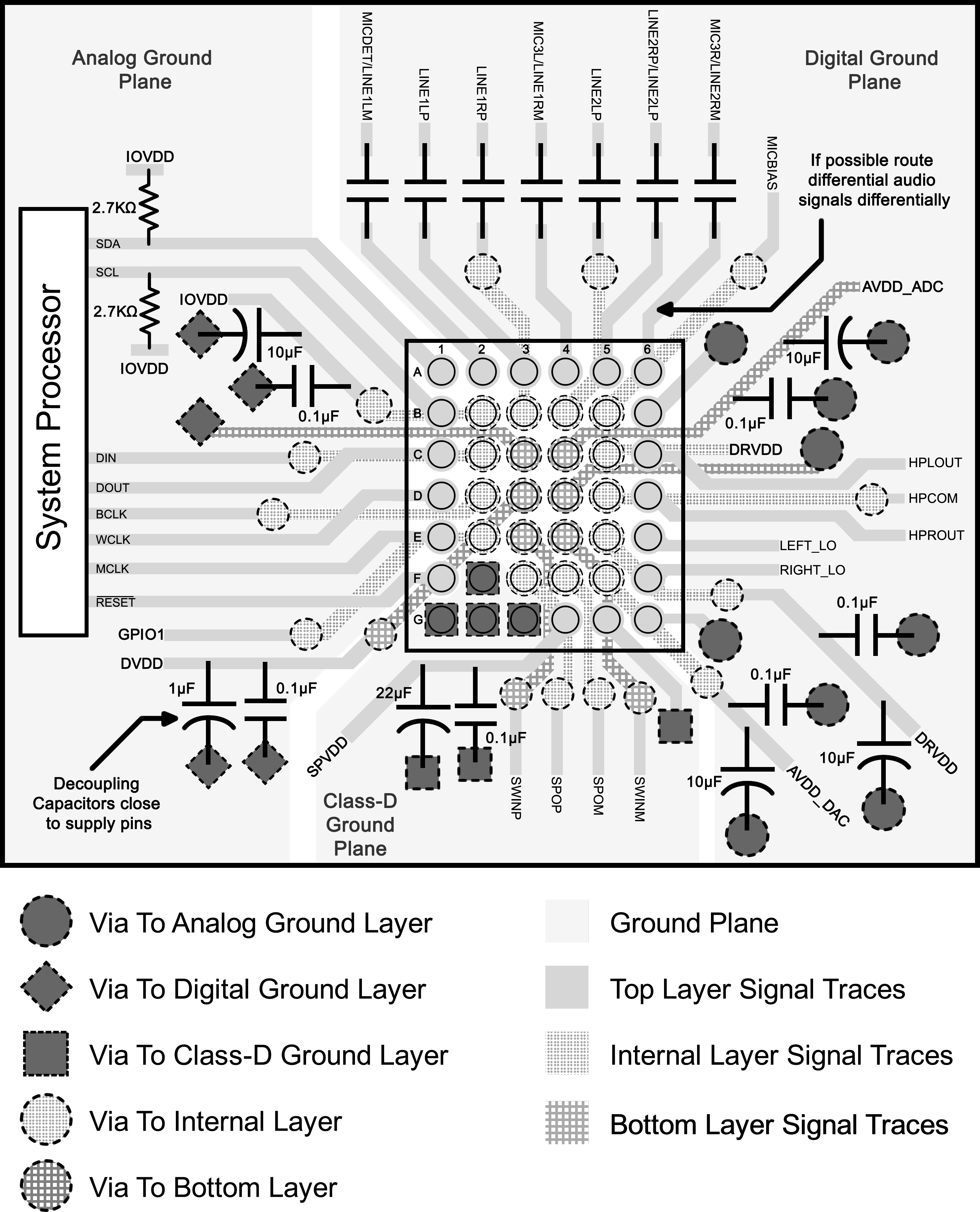
Figure 42. AIC3107 DSBGA Layout Example