SLOS545D November 2008 – December 2014 TLV320AIC3107
UNLESS OTHERWISE NOTED, this document contains PRODUCTION DATA.
- 1 Features
- 2 Applications
- 3 Description
- 4 Simplified Block Diagram
- 5 Revision History
- 6 Description (Continued)
- 7 Pin Configuration and Functions
- 8 Specifications
- 9 Parameter Measurement Information
-
10Detailed Description
- 10.1 Overview
- 10.2 Functional Block Diagram
- 10.3
Feature Description
- 10.3.1 Hardware Reset
- 10.3.2 Digital Audio Data Serial Interface
- 10.3.3 Audio Data Converters
- 10.3.4 Audio Analog Inputs
- 10.3.5 Analog Line Output Drivers
- 10.3.6 Analog High Power Output Drivers
- 10.3.7 Input Impedance and VCM Control
- 10.3.8 General Purpose I/O
- 10.3.9 MICBIAS Generation
- 10.3.10 Class-D Speaker Driver
- 10.3.11 Short Circuit Output Protection
- 10.3.12 Jack and Headset Detection
- 10.4 Device Functional Modes
- 10.5 Programming
- 10.6 Register Maps
- 11Application and Implementation
- 12Power Supply Recommendations
- 13Layout
- 14Device and Documentation Support
- 15Mechanical, Packaging, and Orderable Information
Package Options
Mechanical Data (Package|Pins)
Thermal pad, mechanical data (Package|Pins)
- RSB|40
Orderable Information
8 Specifications
8.1 Absolute Maximum Ratings
over operating free-air temperature range (unless otherwise noted)(1)(2)| MIN | MAX | UNIT | ||
|---|---|---|---|---|
| AVDD_DAC to AVSS_DAC, DRVDD to DRVSS, AVSS_ADC | –0.3 | 3.9 | V | |
| SPVDD to SPVSS | –0.3 | 6.0 | V | |
| AVDD to DRVSS | –0.3 | 3.9 | V | |
| IOVDD to DVSS | –0.3 | 3.9 | V | |
| DVDD to DVSS | –0.3 | 2.5 | V | |
| AVDD_DAC to DRVDD | –0.1 | 0.1 | V | |
| Digital input voltage to DVSS | –0.3 | IOVDD + 0.3 | V | |
| Analog input voltage to AVSS_ADC | –0.3 | AVDD + 0.3 | V | |
| Operating temperature range | –40 | 85 | °C | |
| TJ Max | Junction temperature | 105 | °C | |
| Power dissipation | (TJ Max – TA)/θJA | |||
| Tstg | Storage temperature range | –65 | 105 | °C |
(1) Stresses beyond those listed under Absolute Maximum Ratings may cause permanent damage to the device. These are stress ratings only, and functional operation of the device at these or any other conditions beyond those indicated under Recommended Operating Conditions is not implied. Exposure to absolute-maximum-rated conditions for extended periods may affect device reliability.
(2) ESD compliance tested to EIA/JESD22-A114-B and passed.
8.2 ESD Ratings
| VALUE | UNIT | |||
|---|---|---|---|---|
| V(ESD) | Electrostatic discharge | Human-body model (HBM), per ANSI/ESDA/JEDEC JS-001(1) | ±2300 | V |
| Charged-device model (CDM), per JEDEC specification JESD22-C101(2) | ±1000 | |||
(1) JEDEC document JEP155 states that 500-V HBM allows safe manufacturing with a standard ESD control process.
(2) JEDEC document JEP157 states that 250-V CDM allows safe manufacturing with a standard ESD control process.
8.3 Recommended Operating Conditions
over operating free-air temperature range (unless otherwise noted)| MIN | NOM | MAX | UNIT | ||
|---|---|---|---|---|---|
| AVDD_DAC, DRVDD(1) | Analog supply voltage | 2.7 | 3.3 | 3.6 | V |
| DVDD(1) | Digital core supply voltage | 1.525 | 1.8 | 1.95 | V |
| IOVDD(1) | Digital I/O supply voltage | 1.1 | 1.8 | 3.6 | V |
| SPVDD | Speaker Amplifier supply voltage | 2.7 | 3.6 | 5.5 | V |
| VI | Analog full-scale 0 dB input voltage (DRVDD1 = 3.3 V) (Single Ended) | 0.707 | VRMS | ||
| Stereo line output load resistance | 10 | kΩ | |||
| Stereo headphone output load resistance | 16 | Ω | |||
| Digital output load capacitance | 10 | pF | |||
| TA | Operating free-air temperature | –40 | 85 | °C | |
(1) Analog voltage values are with respect to AVSS_ADC, AVSS_DAC, DRVSS; digital voltage values are with respect to DVSS.
8.4 Thermal Information
| THERMAL METRIC(1) | TLV320AIC3107 | UNIT | ||
|---|---|---|---|---|
| RSB | YZF | |||
| 40 PINS | 42 PINS | |||
| RθJA | Junction-to-ambient thermal resistance | 30.7 | 49.5 | °C/W |
| RθJC(top) | Junction-to-case (top) thermal resistance | 16 | 0.1 | |
| RθJB | Junction-to-board thermal resistance | 4.6 | 7.1 | |
| ψJT | Junction-to-top characterization parameter | 0.2 | 0.8 | |
| ψJB | Junction-to-board characterization parameter | 4.5 | 7 | |
| RθJC(bot) | Junction-to-case (bottom) thermal resistance | 0.9 | n/a | |
(1) For more information about traditional and new thermal metrics, see the IC Package Thermal Metrics application report, SPRA953.
8.5 Dissipation Ratings(1)
| PACKAGE TYPE | TA = 25°C POWER RATING |
DERATING FACTOR | TA = 75°C POWER RATING |
TA = 85°C POWER RATING |
|---|---|---|---|---|
| DSBGA(2) | 1.60 W | 20 mW/°C | 600 mW | 400 mW |
| QFN | 2.35 W | 29.4 mW/° C | 882 mW | 588 mW |
(1) This data was taken using 2 oz. trace and copper pad that is soldered directly to a JEDEC standard 4-layer 3 in × 3 in PCB.
(2) Product Preview
8.6 Electrical Characteristics
At 25°C, AVDD_DAC = 3.3 V, DRVDD = 3.3 V, SPVDD = 5 V, IOVDD = 3.3 V, DVDD = 1.8 V, Fs = 48-kHz, 16-bit audio data(unless otherwise noted)
| PARAMETER | TEST CONDITIONS | MIN | TYP | MAX | UNIT | ||
|---|---|---|---|---|---|---|---|
| AUDIO ADC | |||||||
| Input signal level (0 dB) | Single-ended input | 0.707 | VRMS | ||||
| Signal-to-noise ratio, A-weighted(1)(2) | Fs = 48 ksps, 0 dB PGA gain, Inputs ac-shorted to ground | 80 | 92 | dB | |||
| Dynamic range (2) | Fs = 48 ksps, 0 dB PGA gain, –60 dB full-scale input signal |
91 | dB | ||||
| THD | Total harmonic distortion | Fs = 48 ksps, 0 dB PGA gain, –2dB full-scale 1kHz input signal |
–88 | –70 | dB | ||
| Power supply rejection ratio | 217 Hz signal applied to DRVDD | 49 | dB | ||||
| 1 kHz signal applied to DRVDD | 46 | ||||||
| Gain error | Fs = 48 ksps, 0 dB PGA gain, –2dB full-scale 1kHz input signal |
0.84 | dB | ||||
| Input channel separation | 1 kHz, -2dB full-scale signal, MIC3L to MIC3R | -86 | dB | ||||
| 1 kHz, -2dB full-scale signal, MIC2L to MIC2R | -98 | ||||||
| 1 kHz, -2dB full-scale signal, MIC1L to MIC1R | -75 | ||||||
| ADC programmable gain amplifier maximum gain | 1-kHz input tone | 59.5 | dB | ||||
| ADC programmable gain amplifier step size | 0.5 | dB | |||||
| Input resistance | LINE1L inputs routed to single ADC Input mix attenuation = 0 dB |
20 | kΩ | ||||
| LINE1L inputs routed to single ADC, input mix attenuation = 12 dB |
80 | ||||||
| LINE2L inputs routed to single ADC Input mix attenuation = 0 dB |
20 | ||||||
| LINE2L inputs routed to single ADC, input mix attenuation = 12 dB |
80 | ||||||
| Input level control minimum attenuation setting | 0 | dB | |||||
| Input level control maximum attenuation setting | 12 | dB | |||||
| Input signal level | Differential Input | 1.414 | VRMS | ||||
| Signal-to-noise ratio, A-weighted(1)(2) | Fs = 48 ksps, 0 dB PGA gain, Inputs ac-shorted to ground, Differential Mode | 92 | dB | ||||
| THD | Total harmonic distortion | Fs = 48 ksps, 0 dB PGA gain, –2dB Full-scale 1kHz input signal, Differential Mode | –91 | dB | |||
| ANALOG PASS THROUGH MODE | |||||||
| Input to output switch resistance, (rDS(on)) | LINE1L to LEFT_LOP | 330 | Ω | ||||
| LINE1R to RIGHT_LOP | 330 | ||||||
| SWINP to SWOUTP | 1 | ||||||
| SWINM to SWOUTM | 1 | ||||||
| ADC DIGITAL DECIMATION FILTER, Fs = 48 kHz | |||||||
| Filter gain from 0 to 0.39 Fs | ±0.1 | dB | |||||
| Filter gain at 0.4125 Fs | –0.25 | dB | |||||
| Filter gain at 0.45 Fs | –3 | dB | |||||
| Filter gain at 0.5 Fs | –17.5 | dB | |||||
| Filter gain from 0.55 Fs to 64 Fs | –75 | dB | |||||
| Filter group delay | 17/Fs | s | |||||
| MICROPHONE BIAS | |||||||
| Bias voltage | Programmable setting = 2.0 | 2 | V | ||||
| Programmable setting = 2.5 | 2.3 | 2.5 | 2.7 | ||||
| Programmable setting = DRVDD | DRVDD | ||||||
| Current sourcing | Programmable setting = 2.5V | 4 | mA | ||||
| AUDIO DAC - SINGLE ENDED LINE OUTPUT, LOAD = 10 kΩ | |||||||
| Full-scale output voltage | 0 dB Input full-scale signal, output volume control = 0 dB, Output common mode setting = 1.35 V |
0.707 | Vrms | ||||
| Signal-to-noise ratio, A-weighted | No input signal, output volume control = 0 dB, Output common mode setting = 1.35 V, Fs = 48 kHz |
97 | dB | ||||
| Total harmonic distortion | 0 dB 1 kHz input full-scale signal, Output volume control = 0 dB, Output common mode setting = 1.35 V, Fs = 48 kHz |
-84 | -70 | dB | |||
| DAC Gain Error | 0 dB 1 kHz input full-scale signal, Output volume control = 0 dB, Output common mode setting = 1.35 V, Fs = 48 kHz |
-0.8 | dB | ||||
| AUDIO DAC - SINGLE ENDED HEADPHONE OUTPUT, LOAD = 16 Ω | |||||||
| Full-scale output voltage | 0 dB Input full-scale signal, Output volume control = 0 dB, Output common mode setting = 1.35 V |
0.707 | Vrms | ||||
| Signal-to-noise ratio, A-weighted | No input signal, output volume control = 0 dB, Output common mode setting = 1.35 V, Fs = 48 kHz |
95 | dB | ||||
| No input signal, output volume control = 0 dB, Output common mode setting = 1.35 V, Fs = 48 kHz, 50% DAC Current Boost Mode |
96 | dB | |||||
| Dynamic range, A-weighted | –60 dB 1 kHz input full-scale signal, Output volume control = 0 dB, Output common mode setting = 1.35 V, Fs = 48 kHz |
92 | dB | ||||
| Total harmonic distortion | 0 dB 1 kHz input full-scale signal, Output volume control = 0 dB, Output common mode setting = 1.35 V, Fs = 48 kHz |
-84 | -65 | dB | |||
| Power supply rejection ratio | 217 Hz Signal applied to DRVDD, AVDD_DAC | 41 | dB | ||||
| 1 kHz Signal applied to DRVDD, AVDD_DAC | 44 | ||||||
| DAC channel separation | 0 dB Full-scale input signal between left and right Lineout | 84 | dB | ||||
| DAC Gain Error | 0 dB 1 kHz input full-scale signal, Output volume control = 0 dB, Output common mode setting = 1.35 V, Fs = 48 kHz |
-1 | dB | ||||
| AUDIO DAC - LINEOUT AND HEADPHONE OUT DRIVERS | |||||||
| Output common mode | First option | 1.35 | V | ||||
| Second option | 1.5 | ||||||
| Third option | 1.65 | ||||||
| Fourth option | 1.8 | ||||||
| Output volume control max setting | 9 | dB | |||||
| Output volume control step size | 1 | dB | |||||
| SPEAKER AMPLIFIER OUTPUT, LOAD = 8 Ω | |||||||
| Full-scale output voltage | 1 kHz, 0dB full-scale input signal, Output volume control for left line output = 0 dB, for class-D = 0 dB Output common mode setting = 1.35 V, Fs = 48 kHz |
2.5 | Vrms | ||||
| Output voltage | 1 kHz, 0dB full-scale input signal, Output volume control for left line output = -4.5 dB, for class-D = 6 dB Output common mode setting = 1.35 V, Fs = 48 kHz |
2.875 | Vrms | ||||
| Idle Channel Noise | No input signal, output gain control = 0 dB | -92 | dB | ||||
| Dynamic range, A-weighted | 1 kHz,–60 dB full-scale input signal, Output volume control for left line output = 0 dB, for class-D = 0 dB Output common mode setting = 1.35 V, Fs = 48 kHz |
91 | dB | ||||
| Total harmonic distortion | 1 kHz, 0 dB full-scale input signal, Output volume control for left line output = –4.5 dB, for class-D = 6 dB Output common mode setting = 1.35 V, Fs = 48 kHz, 1 W output power |
1.77% -35 |
dB | ||||
| Total harmonic distortion | 1 kHz, –6 dB full-scale input signal, Output volume control for left line output = –4.5 dB, for class-D = 6 dB Output common mode setting = 1.35 V, Fs = 48 kHz, 250 mW output power |
0.056% -65 |
0.316% -50 |
dB | |||
| Power supply rejection ratio | 217 Hz Signal applied to SPVDD | 37 | dB | ||||
| 1 kHz Signal applied to SPVDD | 33 | ||||||
| Gain Error | 1 kHz, 0 dB input full-scale signal, Output volume control = 0 dB, Output common mode setting = 1.35 V, Fs = 48 kHz |
-1.6 | dB | ||||
| DAC DIGITAL INTERPOLATION – FILTER Fs = 48-ksps | |||||||
| Passband | 0 | 0.45 × Fs | Hz | ||||
| Passband ripple | ±0.06 | dB | |||||
| Transition band | 0.45 × Fs | 0.55 × Fs | Hz | ||||
| Stopband | 0.55 × Fs | 7.5 × Fs | Hz | ||||
| Stopband attenuation | 65 | dB | |||||
| Group delay | 21/Fs | s | |||||
| DIGITAL I/O | |||||||
| VIL | Input low level | –0.3 | 0.3 × IOVDD | V | |||
| VIH | Input high level(3) | IOVDD > 1.6 V | 0.7 × IOVDD | V | |||
| IOVDD < 1.6 V | 1.1 | ||||||
| VOL | Output low level | 0.1 × IOVDD | V | ||||
| VOH | Output high level | 0.8 × IOVDD | V | ||||
| POWER CONSUMPTION, DRVDD, AVDD_DAC = 3.3 V, SPVDD = 5V, DVDD = 1.8 V, IOVDD = 3.3 V | |||||||
| IDRVDD+IAVDD_DAC | RESET Held low | 0.1 | μA | ||||
| IDVDD | 0.2 | ||||||
| IDRVDD+IAVDD_DAC | Mono ADC record, Fs = 8 ksps, I2S Slave, AGC Off, No signal | 2.1 | mA | ||||
| IDVDD | 0.5 | ||||||
| IDRVDD+IAVDD_DAC | Stereo ADC record, Fs = 8 ksps, I2S Slave, AGC Off, No signal | 4.1 | mA | ||||
| IDVDD | 0.6 | ||||||
| IDRVDD+IAVDD_DAC | Stereo ADC record, Fs = 48 ksps, I2S Slave, AGC Off, No signal | 4.3 | mA | ||||
| IDVDD | 2.5 | ||||||
| IDRVDD+IAVDD_DAC | Stereo DAC Playback to Lineout , Analog mixer bypassed Fs = 48 ksps, I2S Slave | 3.5 | mA | ||||
| IDVDD | 2.3 | ||||||
| IDRVDD+IAVDD_DAC | Stereo DAC Playback to Lineout, Fs = 48 ksps, I2S Slave, No signal | 4.9 | mA | ||||
| IDVDD | 2.3 | ||||||
| IDRVDD+IAVDD_DAC | Stereo DAC Playback to stereo single-ended headphone, Fs = 48 ksps, I2S Slave, No signal | 6.7 | mA | ||||
| IDVDD | 2.3 | ||||||
| IDRVDD+IAVDD_DAC | Stereo LINEIN to stereo LINEOUT, No signal | 3.1 | mA | ||||
| IDVDD | 0 | ||||||
| IDRVDD+IAVDD_DAC | Extra power when PLL enabled | 1.4 | mA | ||||
| IDVDD | 0.9 | ||||||
| IDRVDD+IAVDD_DAC | All blocks powered down, Headset detection enabled | 28 | μA | ||||
| IDVDD | 2 | ||||||
| SPVDD | class-D disabled | 200 | nA | ||||
(1) Ratio of output level with 1-kHz full-scale sine-wave input, to the output level with the inputs short circuited, measured A-weighted over a 20-Hz to 20-kHz bandwidth using an audio analyzer.
(2) All performance measurements done with 20-kHz low-pass filter and, where noted, A-weighted filter. Failure to use such a filter may result in higher THD+N and lower SNR and dynamic range readings than shown in the Electrical Characteristics. The low-pass filter removes out-of-band noise, which, although not audible, may affect dynamic specification values.
(3) When IOVDD < 1.6V, minimum VIH is 1.1 V.
8.7 Audio Data Serial Interface Timing Requirements(1)(2)
| IOVDD = 1.1 V | IOVDD = 3.3 V | UNIT | ||||
|---|---|---|---|---|---|---|
| MIN | MAX | MIN | MAX | |||
| I2S/LJF/RJF TIMING IN MASTER MODE, SEE Figure 1 | ||||||
| td(WS) | ADWS/WCLK delay time | 50 | 15 | ns | ||
| td(DO-WS) | ADWS/WCLK to DOUT delay time | 50 | 20 | ns | ||
| td(DO-BCLK) | BCLK to DOUT delay time | 50 | 15 | ns | ||
| ts(DI) | DIN setup time | 10 | 6 | ns | ||
| th(DI) | DIN hold time | 10 | 6 | ns | ||
| tr | Rise time | 30 | 10 | ns | ||
| tf | Fall time | 30 | 10 | ns | ||
| DSP TIMING IN MASTER MODE, SEE Figure 2 | ||||||
| td(WS) | ADWS/WCLK delay time | 50 | 15 | ns | ||
| td(DO-BCLK) | BCLK to DOUT delay time | 50 | 15 | ns | ||
| ts(DI) | DIN setup time | 10 | 6 | ns | ||
| th(DI) | DIN hold time | 10 | 6 | ns | ||
| tr | Rise time | 30 | 10 | ns | ||
| tf | Fall time | 30 | 10 | ns | ||
| I2S/LJF/RJF TIMING IN SLAVE MODE, SEE Figure 3 | ||||||
| tP(BCLK) | BCLK clock period | ns | ||||
| tH(BCLK) | BCLK high period | 70 | 35 | ns | ||
| tL(BCLK) | BCLK low period | 70 | 35 | ns | ||
| ts(WS) | ADWS/WCLK setup time | 10 | 6 | ns | ||
| th(WS) | ADWS/WCLK hold time | 10 | 6 | ns | ||
| td(DO-WS) | ADWS/WCLK to DOUT delay time (for LJF Mode only) | 25 | 35 | ns | ||
| td(DO-BCLK) | BCLK to DOUT delay time | 50 | 20 | ns | ||
| ts(DI) | DIN setup time | 10 | 6 | ns | ||
| th(DI) | DIN hold time | 10 | 6 | ns | ||
| tr | Rise time | 8 | 4 | ns | ||
| tf | Fall time | 8 | 4 | ns | ||
| DSP TIMING IN SLAVE MODE, SEE Figure 4 | ||||||
| tP(BCLK) | BCLK clock period | ns | ||||
| tH(BCLK) | BCLK high period | 70 | 35 | ns | ||
| tL(BCLK) | BCLK low period | 70 | 35 | ns | ||
| ts(WS) | ADWS/WCLK setup time | 10 | 8 | ns | ||
| th(WS) | ADWS/WCLK hold time | 10 | 8 | ns | ||
| td(DO-BCLK) | BCLK to DOUT delay time | 50 | 20 | ns | ||
| ts(DI) | DIN setup time | 10 | 6 | ns | ||
| th(DI) | DIN hold time | 10 | 6 | ns | ||
| tr | Rise time | 8 | 4 | ns | ||
| tf | Fall time | 8 | 4 | ns | ||
(1) All timing specifications are measured at characterization but not tested at final test.
(2) All specifications at 25°C, DVDD = 1.8 V
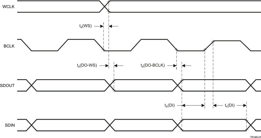 Figure 1. I2S/LJF/RJF Timing in Master Mode
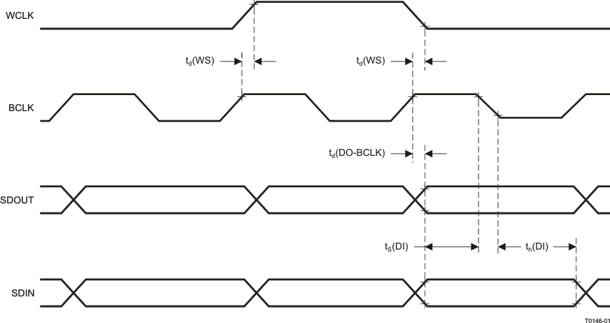 Figure 2. DSP Timing in Master Mode
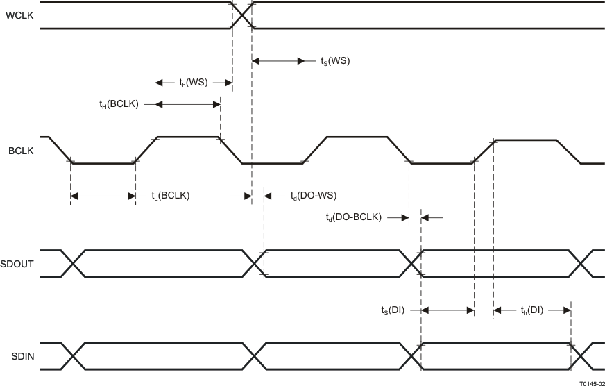 Figure 3. I2S/LJF/RJF Timing in Slave Mode
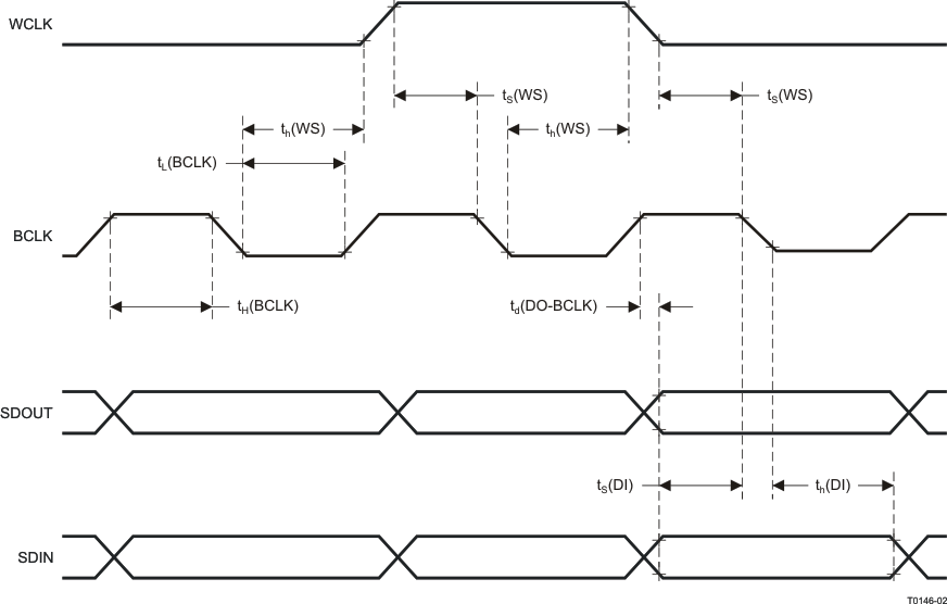 Figure 4. DSP Timing in Slave Mode
8.8 Typical Characteristics
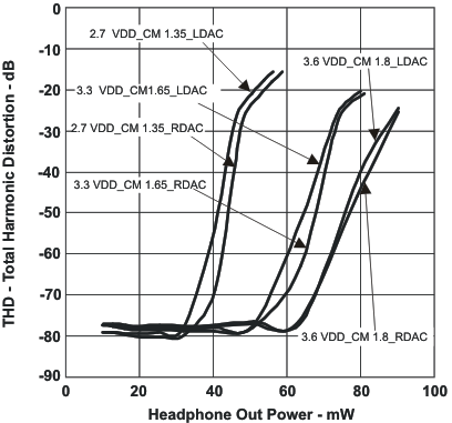 Figure 5. Total Harmonic Distortion vs Headphone Out Power
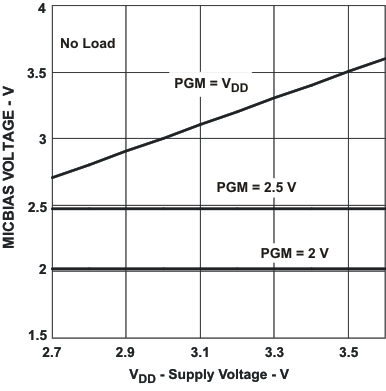 Figure 7. MICBIAS Voltage vs Supply Voltage
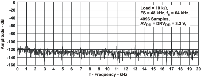 Figure 9. Left DAC FFT
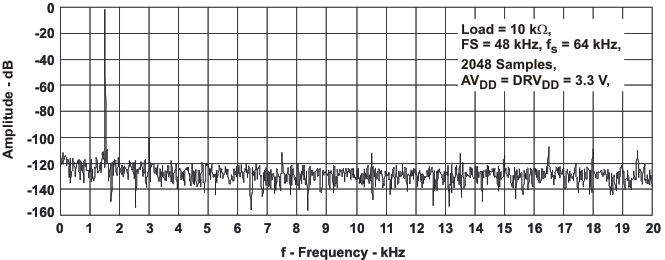 Figure 11. Left ADC FFT
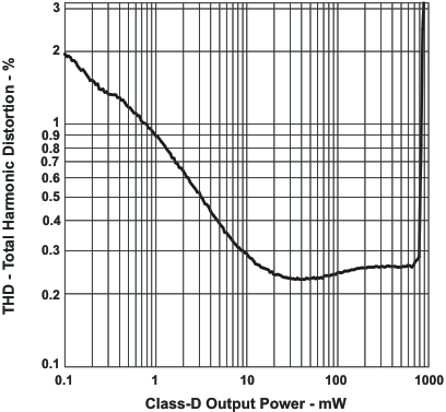 Figure 13. Total Harmonic Distortion vs Class-D Output Power
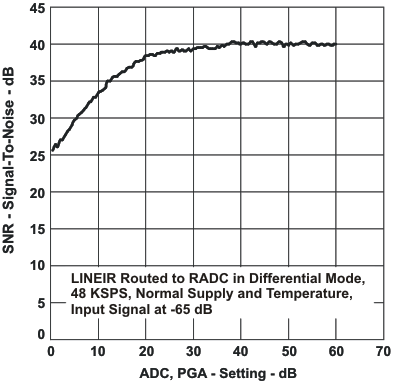 Figure 6. Signal-to-Noise Ratio vs ADC PGA Setting
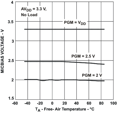 Figure 8. MICBIAS Voltage vs Free-Air Temperature
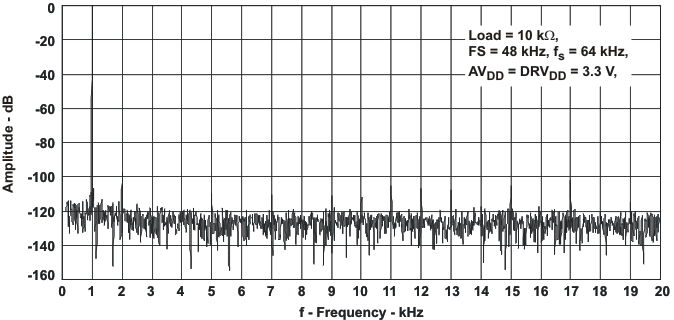 Figure 10. Right DAC FFT
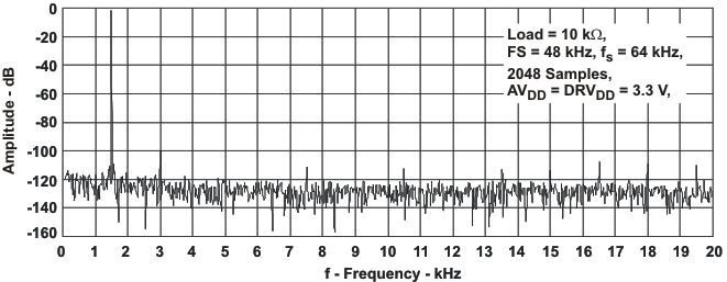 Figure 12. Right ADC FFT