SNOSDA2E august   2020  – july 2023 TLV3604 , TLV3605 , TLV3607

PRODMIX  

  1.   1
  2. Features
  3. Applications
  4. Description
  5. Revision History
  6. Pin Configuration and Functions
    1.     Pin Configurations: TLV3604 and TLV3605
    2. 5.1 Pin Configuration: TLV3607
  7. Specifications
    1. 6.1 Absolute Maximum Ratings
    2. 6.2 ESD Ratings
    3. 6.3 Recommended Operating Conditions
    4. 6.4 Thermal Information
    5. 6.5 Electrical Characteristics (VCCI = VCCO = 2.5 V to 5 V)
    6. 6.6 Typical Characteristics
  8. Detailed Description
    1. 7.1 Overview
    2. 7.2 Functional Block Diagram
    3. 7.3 Feature Description
    4. 7.4 Device Functional Modes
      1. 7.4.1 Rail-to-Rail Inputs
      2. 7.4.2 LVDS Output
  9. Application and Implementation
    1. 8.1 Application Information
      1. 8.1.1 Comparator Inputs
      2. 8.1.2 Capacitive Loads
      3. 8.1.3 Latch Functionality
      4. 8.1.4 Adjustable Hysteresis
    2. 8.2 Typical Application
      1. 8.2.1 Non-Inverting Comparator With Hysteresis
        1. 8.2.1.1 Design Requirements
        2. 8.2.1.2 Detailed Design Procedure
        3. 8.2.1.3 Application Performance Plots
      2. 8.2.2 Optical Receiver
      3. 8.2.3 Logic Clock Source to LVDS Transceiver
      4. 8.2.4 External Trigger Function for Oscilloscopes
  10. Power Supply Recommendations
  11. 10Layout
    1. 10.1 Layout Guidelines
    2. 10.2 Layout Example
  12. 11Device and Documentation Support
    1. 11.1 Device Support
      1. 11.1.1 Development Support
    2. 11.2 Receiving Notification of Documentation Updates
    3. 11.3 Support Resources
    4. 11.4 Trademarks
    5. 11.5 Electrostatic Discharge Caution
    6. 11.6 Glossary
  13. 12Mechanical, Packaging, and Orderable Information

Package Options

Mechanical Data (Package|Pins)
Thermal pad, mechanical data (Package|Pins)
Orderable Information

Optical Receiver

The TLV3604, TLV3605, and TLV3607 can be used in conjunction with a high performance amplifier such as the OPA855 to create an optical receiver as shown in the Figure 8-7. The photo diode is connected to a bias voltage and is being driven with a pulsed laser. The OPA855 takes the current conducting through the diode and translates it into a voltage for a high speed comparator to detect. The TLV3604, TLV3605, and TLV3607 will then output the proper LVDS signal according to the threshold set (VREF2).
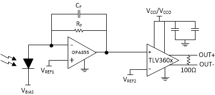
GUID-22F992AA-B421-424D-B7D4-7FDF6563DE19-low.gifFigure 8-7 Optical Receiver