SNVSBU0 October 2020 TLV4062-Q1 , TLV4082-Q1
PRODUCTION DATA
- 1 Features
- 2 Applications
- 3 Description
- 4 Revision History
- 5 Pin Configuration and Functions
- 6 Specifications
- 7 Detailed Description
- 8 Application and Implementation
- 9 Power Supply Recommendations
- 10Layout
- 11Device and Documentation Support
Package Options
Mechanical Data (Package|Pins)
- DBV|6
Thermal pad, mechanical data (Package|Pins)
Orderable Information
3 Description
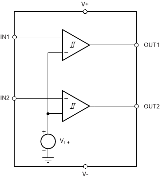
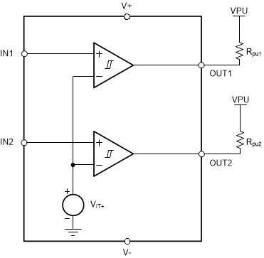
The TLV4062-Q1 and TLV4082-Q1 are a family of high-accuracy, dual-channel comparators featuring low power and small solution size. The IN1 and IN2 inputs include hysteresis to reject brief glitches, thus ensuring stable output operation without false triggering.
The TLV4062-Q1 and TLV4082-Q1 have adjustable INx inputs that can be configured by an external resistor divider pair. When the voltage at the IN1 or IN2 input goes below the falling threshold, OUT1 or OUT2 is driven low, respectively. When IN1 or IN2 rises above the rising threshold, OUT1 or OUT2 goes high, respectively.
The comparators have a very low quiescent current of 2 µA (typical) and provide a precise, space-conscious solution for low-power, voltage monitoring. The TLV4062-Q1 and TLV4082-Q1 operate from 1.5 V to 5.5 V, over the –40°C to +125°C temperature range.
| PART NUMBER | PACKAGE | BODY SIZE (NOM) |
|---|---|---|
| TLV4062-Q1, TLV4082-Q1 | SOT-23 (6) | 2.90 mm × 1.60 mm |
 Block Diagram for
TLV4062-Q1
 Block Diagram for
TLV4082-Q1