SLVS139Y July 1996 – March 2024 TLV431 , TLV431A , TLV431B
PRODUCTION DATA
- 1
- 1 Features
- 2 Applications
- 3 Description
- 4 Pin Configuration and Functions
- 5 Specifications
- 6 Parameter Measurement Information
- 7 Detailed Description
- 8 Applications and Implementation
- 9 Device and Documentation Support
- 10Revision History
- 11Mechanical, Packaging, and Orderable Information
Package Options
Refer to the PDF data sheet for device specific package drawings
Mechanical Data (Package|Pins)
- DBZ|3
- DBV|5
- PK|3
- LP|3
Thermal pad, mechanical data (Package|Pins)
- PK|3
Orderable Information
5.5 Electrical Characteristics for TLV431
at 25°C free-air temperature (unless otherwise
noted)
| PARAMETER | TEST CONDITIONS | TLV431 | UNIT | |||||
|---|---|---|---|---|---|---|---|---|
| MIN | TYP | MAX | ||||||
| VREF | Reference voltage | VKA = VREF, IK=10mA | TA = 25°C | 1.222 | 1.24 | 1.258 | V | |
| TA = full range (1) (see Figure 6-1) | TLV431C | 1.21 | 1.27 | |||||
| TLV431I | 1.202 | 1.278 | ||||||
| TLV431Q | 1.194 | 1.286 | ||||||
| VREF(dev) | VREF deviation over full temperature range(2) | VKA = VREF, IK = 10mA (1) (see Figure 6-1) | TLV431C | 4 | 12 | mV | ||
| TLV431I | 6 | 20 | ||||||
| TLV431Q | 11 | 31 | ||||||
|
Ratio of VREF change in cathode voltage change | VKA = VREF to 6V, IK = 10mA (see Figure 6-2) | -1.5 | -2.7 | mV/V | |||
| Iref | Reference terminal current | IK = 10mA, R1 = 10kΩ, R2 = open (see Figure 6-2) | 0.15 | 0.5 | µA | |||
| Iref(dev) | Iref deviation over full temperature range(2) | IK = 10mA, R1 =10kΩ, R2 = open (1) (see Figure 6-2) | TLV431C | 0.05 | 0.3 | µA | ||
| TLV431I | 0.1 | 0.4 | ||||||
| TLV431Q | 0.15 | 0.5 | ||||||
| IK(min) | Minimum cathode current for regulation | VKA = VREF (see Figure 6-1) | TLV431C/I | 55 | 80 | µA | ||
| TLV431Q | 55 | 100 | ||||||
| IK(off) | Off-state cathode current | VREF = 0, VKA = 6V (see Figure 6-3) | 0.001 | 0.1 | µA | |||
| |zKA| | Dynamic impedance(3) | VKA = VREF, f ≤ 1kHz, IK = 0.1mA to 15mA (see Figure 6-1) | 0.25 | 0.4 | Ω | |||
(1) Full temperature ranges are
–40°C to 125°C for TLV431Q, –40°C to 85°C for TLV431I, and 0°C to 70°C for
TLV431C.
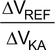
(2) The deviation parameters
VREF(dev) and Iref(dev) are defined as the differences
between the maximum and minimum values obtained over the rated temperature
range. The average full-range temperature coefficient of the reference input
voltage, αVREF, is defined as:
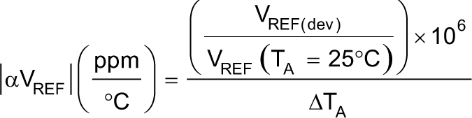 where ΔTA is the rated operating free-air temperature range of
the device. αVREF can be positive or negative, depending on whether
minimum VREF or maximum VREF, respectively, occurs at the
lower temperature.
where ΔTA is the rated operating free-air temperature range of
the device. αVREF can be positive or negative, depending on whether
minimum VREF or maximum VREF, respectively, occurs at the
lower temperature.
(3) The dynamic impedance is
defined as 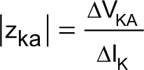 . When the
device is operating with two external resistors (see Figure 6-2), the total dynamic impedance of the circuit is defined as:
. When the
device is operating with two external resistors (see Figure 6-2), the total dynamic impedance of the circuit is defined as:
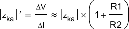
. When the
device is operating with two external resistors (see Figure 6-2), the total dynamic impedance of the circuit is defined as: