SLUSDR2A December   2020  – January 2023 TLV62595

PRODUCTION DATA  

  1. Features
  2. Applications
  3. Description
  4. Revision History
  5. Pin Configuration and Functions
  6. Specifications
    1. 6.1 Absolute Maximum Ratings
    2. 6.2 ESD Ratings
    3. 6.3 Recommended Operating Conditions
    4. 6.4 Thermal Information
    5. 6.5 Electrical Characteristics
    6. 6.6 Typical Characteristics
  7. Detailed Description
    1. 7.1 Overview
    2. 7.2 Functional Block Diagram
    3. 7.3 Feature Description
      1. 7.3.1 Pulse Width Modulation (PWM) Operation
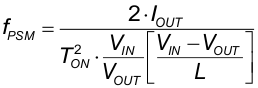
      2. 7.3.2 Power Save Mode (PSM) Operation
      3. 7.3.3 Minimum Duty Cycle and 100% Mode Operation
      4. 7.3.4 Soft Start
      5. 7.3.5 Switch Current Limit and HICCUP Short-Circuit Protection
      6. 7.3.6 Undervoltage Lockout
      7. 7.3.7 Thermal Shutdown
    4. 7.4 Device Functional Modes
      1. 7.4.1 Enable, Disable and Output Discharge
      2. 7.4.2 Power Good
  8. Application and Implementation
    1. 8.1 Application Information
    2. 8.2 Typical Application
      1. 8.2.1 Design Requirements
      2. 8.2.2 Detailed Design Procedure
        1. 8.2.2.1 Custom Design With WEBENCH® Tools
        2. 8.2.2.2 Setting The Output Voltage
        3. 8.2.2.3 Output Filter Design
        4. 8.2.2.4 Inductor Selection
        5. 8.2.2.5 Capacitor Selection
      3. 8.2.3 Application Curves
    3. 8.3 Power Supply Recommendations
    4. 8.4 Layout
      1. 8.4.1 Layout Guidelines
      2. 8.4.2 Layout Example
        1. 8.4.2.1 Thermal Considerations
  9. Device and Documentation Support
    1. 9.1 Device Support
      1. 9.1.1 Third-Party Products Disclaimer
      2. 9.1.2 Development Support
        1. 9.1.2.1 Custom Design With WEBENCH® Tools
    2. 9.2 Documentation Support
      1. 9.2.1 Related Documentation
    3. 9.3 Receiving Notification of Documentation Updates
    4. 9.4 Support Resources
    5. 9.5 Trademarks
    6. 9.6 Electrostatic Discharge Caution
    7. 9.7 Glossary
  10. 10Mechanical, Packaging, and Orderable Information

Package Options

Mechanical Data (Package|Pins)
Thermal pad, mechanical data (Package|Pins)
Orderable Information

Power Save Mode (PSM) Operation

To maintain high efficiency at light loads, the device enters power save mode (PSM) at the boundary to discontinuous conduction mode (DCM). This happens when the output current becomes smaller than half of the ripple current of the inductor. The device operates now with a fixed on-time and the switching frequency further decreases proportionally to the load current. It can be calculated as:

Equation 2. GUID-B2633458-6FE6-46FF-B566-79E59DB31E41-low.gif

In PSM, the output voltage rises slightly above the nominal target, which can be minimized using larger output capacitance. At duty cycles larger than 90%, the device may not enter PSM. The device maintains output regulation in PWM mode.