SNOSD29E December   2016  – April 2018 TLV8541 , TLV8542 , TLV8544

UNLESS OTHERWISE NOTED, this document contains PRODUCTION DATA.  

  1. Features
  2. Applications
  3. Description
    1.     Device Images
      1.      Low Power PIR Motion Detector
  4. Revision History
  5. Description (continued)
  6. Pin Configuration and Functions
    1.     Pin Functions: TLV8541 DBV
    2.     Pin Functions: TLV8542 D & RUG
    3.     Pin Functions: TLV8544 PW & D
  7. Specifications
    1. 7.1 Absolute Maximum Ratings
    2. 7.2 ESD Ratings
    3. 7.3 Recommended Operating Conditions
    4. 7.4 Thermal Information
    5. 7.5 Electrical Characteristics
    6. 7.6 Typical Characteristics
  8. Detailed Description
    1. 8.1 Overview
    2. 8.2 Functional Block Diagram
    3. 8.3 Feature Description
    4. 8.4 Device Functional Modes
      1. 8.4.1 Rail-To-Rail Input
      2. 8.4.2 Supply Current Changes Over Common Mode
      3. 8.4.3 Design Optimization With Rail-To-Rail Input
      4. 8.4.4 Design Optimization for Nanopower Operation
      5. 8.4.5 Common-Mode Rejection
      6. 8.4.6 Output Stage
      7. 8.4.7 Driving Capacitive Load
  9. Application and Implementation
    1. 9.1 Application Information
    2. 9.2 Typical Application: Battery-Powered Wireless PIR Motion Detectors
      1. 9.2.1 Design Requirements
      2. 9.2.2 Detailed Design Procedure
        1. 9.2.2.1 Calculation of the Cutoff Frequencies and Gain of Stage A:
        2. 9.2.2.2 Calculation of the Cutoff Frequencies and Gain of Stage B
        3. 9.2.2.3 Calculation of the Total Gain of Stages A and B
        4. 9.2.2.4 Window Comparator Stage
        5. 9.2.2.5 Reference Voltages
      3. 9.2.3 Application Curve
    3. 9.3 Typical Application: 60-Hz Twin T Notch Filter
      1. 9.3.1 Design Requirements
      2. 9.3.2 Detailed Design Procedure
      3. 9.3.3 Application Curve
    4. 9.4 Dos and Don'ts
  10. 10Power Supply Recommendations
  11. 11Layout
    1. 11.1 Layout Guidelines
    2. 11.2 Layout Example
  12. 12Device and Documentation Support
    1. 12.1 Device Support
      1. 12.1.1 Development Support
    2. 12.2 Documentation Support
      1. 12.2.1 Related Documentation
    3. 12.3 Related Links
    4. 12.4 Receiving Notification of Documentation Updates
    5. 12.5 Community Resources
    6. 12.6 Trademarks
    7. 12.7 Electrostatic Discharge Caution
    8. 12.8 Glossary
  13. 13Mechanical, Packaging, and Orderable Information

Package Options

Mechanical Data (Package|Pins)
Thermal pad, mechanical data (Package|Pins)
Orderable Information

Driving Capacitive Load

The TLV854x is internally compensated for stable unity-gain operation, with a 8-kHz typical gain bandwidth. However, the unity-gain follower is the most sensitive configuration-to-capacitive load. The combination of a capacitive load placed directly on the output of an amplifier along with the output impedance of the amplifier creates a phase lag, which reduces the phase margin of the amplifier. If the phase margin is significantly reduced, the response is under-damped, which causes peaking in the transfer and, when there is too much peaking, the op amp might start oscillating.

In order to drive heavy (> 50 pF) capacitive loads, use an isolation resistor, RISO, as shown in Figure 31. By using this isolation resistor, the capacitive load is isolated from the output of the amplifier. The larger the value of RISO, the more stable the amplifier will be. If the value of RISO is sufficiently large, the feedback loop is stable, independent of the value of CL. However, larger values of RISO (e.g. 50 kΩ) result in reduced output swing and reduced output current drive.
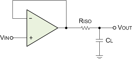
TLV8544 TLV8542 TLV8541 CAP-DRIV-BD_SNOSD29.gifFigure 31. Resistive Isolation of Capacitive Load