SBOS486I July 2009 – December 2018 TMP303
PRODUCTION DATA.
- 1 Features
- 2 Applications
- 3 Description
- 4 Revision History
- 5 Device Options
- 6 Pin Configuration and Functions
- 7 Specifications
- 8 Detailed Description
- 9 Application and Implementation
- 10Power Supply Recommendations
- 11Layout
- 12Device and Documentation Support
- 13Mechanical, Packaging, and Orderable Information
Package Options
Mechanical Data (Package|Pins)
- DRL|6
Thermal pad, mechanical data (Package|Pins)
Orderable Information
8.3.2 TMP303 Power Up and Timing
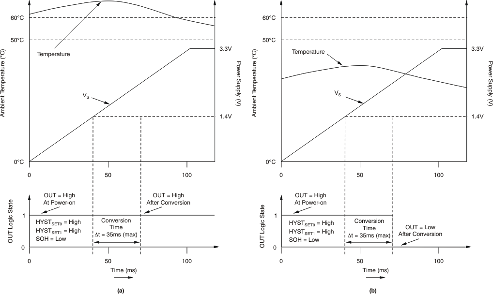
At device power up, the TMP303 exerts OUT = high, and typically requires 26 ms to return to a low state only if the temperature falls within the hysteresis window set by HYSTSET0 and HYSTSET1.
The tolerance of the thermal response time is largely a result of the differences in conversion time, which varies from 20 ms to 35 ms; likewise, this conversion does not take place after a power cycle until the supply voltage has reached a level of at least 1.4 V. This sequence is illustrated in Figure 11.
 Figure 11. TMP303A Start-Up Delay vs Output Voltage (HYSTSET0 = HYSTSET1 = VS)
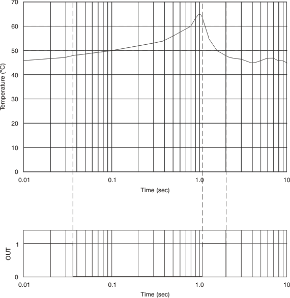
 After the TMP303 powers up, all successive thermal response results for the device are achieved in a time frame of 0.985 s to 1 s. This period is the minimum time frame required for the push-pull output (OUT) to change its state from high to low (or conversely) when the device is active.
A maximum low output voltage is defined as a voltage level equivalent to (0.2 × VS); likewise, a minimum high-output voltage is defined as (0.8 × VS). The timing associated with start-up time and conversion is shown in Figure 12.
 Figure 12. TMP303A Start-Up and Conversion Timing (HYSTSET0 = HYSTSET1 = VS)