SPRS727C August 2012 – April 2014 TMS320C5517
PRODUCTION DATA.
- 1Device Overview
- 2Revision History
- 3Device Comparison
-
4Terminal Configuration and Functions
- 4.1 Pin Diagram
- 4.2
Signal Descriptions
- 4.2.1 Oscillator and PLL
- 4.2.2 Real-Time Clock (RTC)
- 4.2.3 RESET, Interrupts, and JTAG
- 4.2.4 External Memory Interface (EMIF)
- 4.2.5 Inter-Integrated Circuit (I2C)
- 4.2.6 Inter-IC Sound (I2S)
- 4.2.7 Multichannel Buffered Serial Port (McBSP)
- 4.2.8 Multichannel Serial Port Interface (McSPI)
- 4.2.9 Serial Peripheral Interface (SPI)
- 4.2.10 Universal Asynchronous Receiver and Transmitter (UART)
- 4.2.11 Universal Serial Bus (USB) 2.0
- 4.2.12 Universal Host-Port Interface (UHPI)
- 4.2.13 MultiMedia Card (MMC)
- 4.2.14 Successive Approximation (SAR) Analog-to-Digital Converter (ADC)
- 4.2.15 General-Purpose Input and Output (GPIO)
- 4.2.16 Regulators and Power Management
- 4.2.17 Supply Voltage
- 4.2.18 Ground
- 4.3
Pin Multiplexing
- 4.3.1 UHPI, SPI, UART, I2S2, I2S3, and GP[31:27, 20:12] Pin Multiplexing [EBSR.PPMODE Bits]
- 4.3.2 MMC1, McSPI, and GP[11:6] Pin Multiplexing [EBSR.SP1MODE Bits]
- 4.3.3 MMC0, I2S0, McBSP, and GP[5:0] Pin Multiplexing [EBSR.SP0MODE Bits]
- 4.3.4 EMIF EM_A[20:15] and GP[26:21] Pin Multiplexing [EBSR.Axx_MODE bits]
- 4.4 Connections for Unused Signals
-
5Specifications
- 5.1 Absolute Maximum Ratings
- 5.2 Recommended Operating Conditions
- 5.3 Electrical Characteristics
- 5.4 Handling Ratings
- 5.5 Thermal Characteristics
- 5.6 Power-On Hours
- 5.7
Timing and Switching Characteristics
- 5.7.1 Parameter Information
- 5.7.2 Power Supplies
- 5.7.3
Reset
- 5.7.3.1 Power-On Reset (POR) Circuits
- 5.7.3.2 Pin Behavior at Reset
- 5.7.3.3 Reset Electrical Data and Timing
- 5.7.3.4 Configurations at Reset
- 5.7.3.5
Configurations After Reset
- 5.7.3.5.1 External Bus Selection Register (EBSR)
- 5.7.3.5.2 LDO Control Register [7004h]
- 5.7.3.5.3 EMIF and USB System Control Registers (ESCR and USBSCR) [1C33h and 1C32h]
- 5.7.3.5.4 Peripheral Clock Gating Control Registers (PCGCR1 and PCGCR2) [1C02h and 1C03h]
- 5.7.3.5.5 Pullup and Pulldown Inhibit Registers (PUDINHIBR1, 2, 3, 4, 5, 6, and 7) [1C17h, 1C18h, 1C19h, 1C4Ch, 1C4Dh, 1C4Fh, and 1C50h, respectively]
- 5.7.3.5.6 Output Slew Rate Control Register (OSRCR) [1C16h]
- 5.7.4
Clock Specifications
- 5.7.4.1 Recommended Clock and Control Signal Transition Behavior
- 5.7.4.2 Clock Considerations
- 5.7.4.3 PLLs
- 5.7.4.4 Input and Output Clocks Electrical Data and Timing
- 5.7.4.5 Wake-up Events, Interrupts, and XF
- 5.7.5 Direct Memory Access (DMA) Controller
- 5.7.6 External Memory Interface (EMIF)
- 5.7.7 General-Purpose Input/Output (GPIO)
- 5.7.8 Inter-Integrated Circuit (I2C)
- 5.7.9 Inter-IC Sound (I2S)
- 5.7.10 Multichannel Serial Port Interface (McSPI)
- 5.7.11 Multichannel Buffered Serial Port (McBSP)
- 5.7.12 Multimedia Card and Secure Digital (eMMC, MMC, SD, and SDHC)
- 5.7.13 Real-Time Clock (RTC)
- 5.7.14 SAR ADC (10-Bit)
- 5.7.15 Serial Port Interface (SPI)
- 5.7.16 Timers
- 5.7.17 Universal Asynchronous Receiver and Transmitter (UART)
- 5.7.18 Universal Host-Port Interface (UHPI)
- 5.7.19 Universal Serial Bus (USB) 2.0 Controller
- 5.7.20 Emulation and Debug
- 5.7.21 IEEE 1149.1 JTAG
-
6Detailed Description
- 6.1 CPU
- 6.2
Memory
- 6.2.1 Internal Memory
- 6.2.2 External Memory
- 6.2.3 Memory Map
- 6.2.4
Register Map
- 6.2.4.1 DMA Peripheral Register Description
- 6.2.4.2 EMIF Peripheral Register Description
- 6.2.4.3 GPIO Peripheral Register Description
- 6.2.4.4 I2C Peripheral Register Description
- 6.2.4.5 I2S Peripheral Register Description
- 6.2.4.6 McBSP Peripheral Register Descriptions
- 6.2.4.7 McSPI Peripheral Register Descriptions
- 6.2.4.8 MMC and SD Peripheral Register Description
- 6.2.4.9 RTC Peripheral Register Description
- 6.2.4.10 SAR ADC Peripheral Register Description
- 6.2.4.11 SPI Peripheral Register Descriptions
- 6.2.4.12 System Registers
- 6.2.4.13 Timers Peripheral Register Description
- 6.2.4.14 UART Peripheral Register Description
- 6.2.4.15 UHPI Peripheral Register Descriptions
- 6.2.4.16 USB2.0 Peripheral Register Descriptions
- 6.3 Identification
- 6.4 Boot Modes
- 7Device and Documentation Support
- 8Mechanical Packaging and Orderable Information
Package Options
Refer to the PDF data sheet for device specific package drawings
Mechanical Data (Package|Pins)
- ZCH|196
Thermal pad, mechanical data (Package|Pins)
Orderable Information
5 Specifications
For the device maximum operating frequency, see Section 7.1.2, Device Nomenclature.
5.1 Absolute Maximum Ratings
Over Operating Case Temperature Range (Unless Otherwise Noted)(1)| Supply voltage ranges: | Digital Core (CVDD, CVDDRTC, USB_VDD1P3)(2) | –0.5 V to 1.7 V | |
| I/O, 1.8 V, 2.75 V, 3.3 V (DVDDIO, DVDDEMIF, DVDDRTC) 3.3V USB supplies USB PHY (USB_VDDOSC, USB_VDDPLL, USB_VDDA3P3)(2) | –0.5 V to 4.2 V | ||
| LDOI | –0.5 V to 4.2 V | ||
| Analog, 1.3 V (VDDA_PLL, USB_VDDA1P3, VDDA_ANA)(2) | –0.5 V to 1.7 V | ||
| Input and Output voltage ranges: | VI I/O, All pins with DVDDIO or DVDDEMIF or USB_VDDOSC or USB_VDDPLL or USB_VDDA3P3 as supply source | –0.5 V to 4.2 V | |
| VO I/O, All pins with DVDDIO or DVDDEMIF or USB_VDDOSC or USB_VDDPLLor USB_VDDA3P3 as supply source | –0.5 V to 4.2 V | ||
| RTC_XI and RTC_XO | –0.5 V to 1.7 V | ||
| VI and VO, GPAIN[0] | –0.5 V to 4.2 V | ||
| VI and VO, GPAIN[3:1] | –0.5 V to 1.7 V | ||
| VO, BG_CAP | –0.5 V to 1.7 V | ||
| ANA_LDOO, DSP_LDOO, and USB_LDOO | –0.5 V to 1.7 V | ||
| USB_VBUS Input | 0 V to 5.5 V | ||
| Operating case temperature ranges, Tc: | Commercial Temperature (default) | -10°C to 70°C | |
| Industrial Temperature | -40°C to 85°C | ||
5.2 Recommended Operating Conditions
| MIN | NOM | MAX | UNIT | ||||
|---|---|---|---|---|---|---|---|
| CVDD | Supply voltage, Digital Core Slew rate < 200 µs for full swing |
75 MHz | 0.998 | 1.05 | 1.15 | V | |
| 175 MHz | 1.24 | 1.3 | 1.43 | V | |||
| 200 MHz | 1.33 | 1.4 | 1.47 | V | |||
| Core Supplies | CVDDRTC | Supply voltage, RTC and RTC OSC | 32.768 kHz | 0.998 | CVDD | V | |
| USB_VDD1P3 | Supply voltage, Digital USB | 1.24 | 1.3 | 1.43 | V | ||
| USB_VDDA1P3 | Supply voltage, 1.3 V Analog USB | 1.24 | 1.3 | 1.43 | V | ||
| VDDA_ANA | Supply voltage, 1.3 V SAR and Pwr Mgmt | 1.24 | 1.3 | 1.43 | V | ||
| VDDA_PLL | Supply voltage, System PLL | 1.24 | 1.3 | 1.43 | V | ||
| USB_VDDPLL | Supply voltage, 3.3 V USB PLL | 2.97 | 3.3 | 3.63 | V | ||
| I/O Supplies | DVDDIO DVDDEMIF DVDDRTC |
Supply voltage, I/O, 3.3 V | 2.97 | 3.3 | 3.63 | V | |
| Supply voltage, I/O, 2.75 V | 2.48 | 2.75 | 3.02 | V | |||
| Supply voltage, I/O, 1.8 V | 1.65 | 1.8 | 1.98 | V | |||
| USB_VDDOSC | Supply voltage, I/O, 3.3 V USB OSC | 2.97 | 3.3 | 3.63 | V | ||
| USB_VDDA3P3 | Supply voltage, I/O, 3.3 V Analog USB PHY | 2.97 | 3.3 | 3.63 | V | ||
| LDOI | Supply voltage, Analog Pwr Mgmt and LDO Inputs | 1.8 | 3.6 | V | |||
| GND | VSS | Supply ground, Digital I/O | 0 | 0 | 0 | V | |
| VSSRTC | Supply ground, RTC | ||||||
| USB_VSSOSC | Supply ground, USB OSC | ||||||
| USB_VSSPLL | Supply ground, USB PLL | ||||||
| USB_VSSA3P3 | Supply ground, 3.3 V Analog USB PHY | ||||||
| USB_VSSA1P3 | Supply ground, USB 1.3 V Analog USB PHY | ||||||
| USB_VSSREF | Supply ground, USB Reference Current | ||||||
| VSSA_PLL | Supply ground, System PLL | ||||||
| USB_VSS1P3 | Supply ground, 1.3 V Digital USB PHY | ||||||
| VSSA_ANA | Supply ground, SAR and Pwr Mgmt | ||||||
| VIH(1) | High-level input voltage, 3.3, 2.75, 1.8 V I/O (except GPAIN[3:0] pins) (2) | 0.7 * DVDD | DVDD + 0.3 | V | |||
| VIL(1) | Low-level input voltage, 3.3, 2.75, 1.8 V I/O (except GPAIN[3:0] pins) (2) | -0.3 | 0.3 * DVDD | V | |||
| VIN | Input voltage, GPAIN0 pin(3) | -0.3 | 3.6 | V | |||
| Input voltage, GPAIN[3:1] pins | -0.3 | VDDA_ANA + 0.3 | V | ||||
| Tc | Operating case temperature | Commercial (default) | -10 | 70 | °C | ||
| Industrial | -40 | 85 | °C | ||||
| FSYSCLK | DSP Operating Frequency (SYSCLK) | 1.05 V | 0 | 75 | MHz | ||
| 1.3 V | 0 | 175 | MHz | ||||
| 1.4 V | 0 | 200 | MHz | ||||
5.3 Electrical Characteristics
5.3.1 Power Consumption
NOTE
Power consumption on this device depends on several operating parameters such as operating voltage, operating frequency, and temperature. Power consumption also varies by end applications that determine the overall processor, CPU, and peripheral activity. For more specific power consumption details, see Estimating Power Consumption on the TMS320C5517 Digital Signal Processor [literature number SPRABV3]. This document includes a spreadsheet for estimating power based on parameters that closely resemble the end application to generate a realistic estimate of power consumption on this device based on use-case and operating conditions.
5.3.2 Electrical Characteristics
Over Recommended Ranges of Supply Voltage and Operating Temperature (Unless Otherwise Noted)| PARAMETER | TEST CONDITIONS (1) | MIN | TYP | MAX | UNIT | ||
|---|---|---|---|---|---|---|---|
| VOH | Full speed: USB_DN and USB_DP(7) | 2.8 | USB_VDDA3P3 | V | |||
| High speed: USB_DN and USB_DP(7) | 360 | 440 | mV | ||||
| High-level output voltage, 3.3, 2.75, 1.8 V I/O (except GPAIN[3:0] pins) | IO = IOH | 0.8 * DVDD | V | ||||
| High-level output voltage, GPAIN[3:1] pins | IO = IOH | 0.8 * VDDA_ANA | V | ||||
| VOL | Full speed: USB_DN and USB_DP(7) | 0.0 | 0.3 | V | |||
| High speed: USB_DN and USB_DP(7) | –10 | 10 | mV | ||||
| Low-level output voltage, 3.3, 2.75, 1.8V I/O (except I2C and GPAIN[3:0] pins) | IO = IOL | 0.2 * DVDD | V | ||||
| Low-level output voltage, I2C pins(3) | VDD > 2 V, IOL = 3 mA | 0 | 0.4 | V | |||
| Low-level output voltage, GPAIN[3:0] pins | IO = IOL | 0.2 * VDDA_ANA | V | ||||
| VHYS | Input hysteresis(2) | DVDD = 3.3 V | 162 | mV | |||
| DVDD = 1.8 V | 122 | mV | |||||
| VLDO | USB_LDOO voltage | 1.24 | 1.3 | 1.43 | V | ||
| ANA_LDOO voltage | 1.24 | 1.3 | 1.43 | V | |||
| DSP_LDOO voltage | DSP_LDO_V bit in the LDOCNTL register = 1 | 1.24 | 1.3 | 1.43 | V | ||
| DSP_LDO_V bit in the LDOCNTL register = 0 | 0.998 | 1.05 | 1.15 | V | |||
| ISD | DSP_LDO shutdown current(6) | LDOI = VMIN | 250 | mA | |||
| ANA_LDO shutdown current(6) | LDOI = VMIN | 4 | mA | ||||
| USB_LDO shutdown current(6) | LDOI = VMIN | 25 | mA | ||||
| IILPU(8)(10) | Input current [DC] (except WAKEUP, I2C, and GPAIN[3:0] pins) | Input only pin, internal pulldown or pullup disabled | –5 | +5 | µA | ||
| DVDD = 3.3 V with internal pullup enabled(4) | –59 to –161 |
µA | |||||
| DVDD = 1.8 V with internal pullup enabled(4) | –14 to –44 | µA | |||||
| IIHPD(8)(10) | Input current [DC] (except WAKEUP, I2C, and GPAIN[3:0] pins) | Input only pin, internal pulldown or pullup disabled | –5 | +5 | µA | ||
| DVDD = 3.3 V with internal pulldown enabled(4) | 52 to 158 | µA | |||||
| DVDD = 1.8 V with internal pulldown enabled(4) | 11 to 35 | µA | |||||
| IIH/ IIL(10) |
Input current [DC], ALL pins | VI = VSS to DVDD with internal pullups and pulldowns disabled. | –5 | +5 | µA | ||
| IOH(10) | High-level output current [DC] | All Pins (except USB, EMIF, CLKOUT, and GPAIN[3:0] pins) | –4 | mA | |||
| EMIF pins | DVDD = 3.3 V | –6 | mA | ||||
| DVDD = 1.8 V | –5 | mA | |||||
| CLKOUT pin | DVDD = 3.3 V | –6 | mA | ||||
| DVDD = 1.8 V | –4 | mA | |||||
| GPAIN[3:1] pins (GPAIN0 is open-drain and cannot drive high) |
DVDD = VDDA_ANA = 1.3 V, External Regulator(5) |
–4 | mA | ||||
| DVDD = VDDA_ANA = 1.3 V, Internal Regulator(5) |
–100 | µA | |||||
| IOL(10) | Low-level output current [DC] | All Pins (except USB, EMIF, CLKOUT, and GPAIN[3:0] pins) | +4 | mA | |||
| EMIF pins | DVDD = 3.3 V | +6 | mA | ||||
| DVDD = 1.8 V | +5 | mA | |||||
| CLKOUT pin | DVDD = 3.3 V | +6 | mA | ||||
| DVDD = 1.8 V | +4 | mA | |||||
| GPAIN[3:0] | DVDD = VDDA_ANA = 1.3 V, external regulator | +4 | mA | ||||
| DVDD = VDDA_ANA = 1.3 V, internal regulator(5) | +4 | mA | |||||
| IOZ(9) | I/O Off-state output current | All Pins (except USB and GPAIN[3:0]) | –10 | +10 | µA | ||
| GPAIN[3:0] pins | –10 | +10 | µA | ||||
| IOLBH(11) | Bus Holder pull low current when CVDD is powered "OFF" | Supply voltage, I/O, 3.3 V | 2.2 | mA | |||
| Supply voltage, I/O, 2.75 V | 1.6 | mA | |||||
| Supply voltage, I/O, 1.8 V | 0.72 | mA | |||||
| IOHBH(11) | Bus Holder pull high current when CVDD is powered "OFF" | Supply voltage, I/O, 3.3 V | –1.3 | mA | |||
| Supply voltage, I/O, 2.75 V | –0.97 | mA | |||||
| Supply voltage, I/O, 1.8 V | –0.46 | mA | |||||
| VDDA_PLL = 1.3 V Room Temp, Phase detector = 12 MHz, VCO = 125 MHz |
0.93 | ||||||
| I | Analog PLL (VDDA_PLL) supply current | VDDA_PLL = 1.3 V Room Temp, Phase detector = 12 MHz, VCO = 175 MHz |
1.23 | mA | |||
| VDDA_PLL = 1.3 V Room Temp, Phase detector = 12 MHz, VCO = 200 MHz |
1.54 | ||||||
| SAR Analog (VDDA_ANA) supply current | VDDA_ANA = 1.3 V, SAR clock = 2 MHz, Temp (70 °C) |
1 | mA | ||||
| CI | Input capacitance | 4 | pF | ||||
| Co | Output capacitance | 4 | pF | ||||
5.4 Handling Ratings
| MIN | MAX | UNIT | ||
|---|---|---|---|---|
| Tstg | Storage temperature range (default) | –65 | 150 | ºC |
| Electrostatic Discharge (ESD) Stress Voltage(1) | Human Body Model (HBM)(2) | 0 | >1000 | V |
| Charged Device Model (CDM)(3) | 0 | >250 | V |
Section 5.5 shows the thermal resistance characteristics for the PBGA–ZCH mechanical package.
5.5 Thermal Characteristics
over operating free-air temperature range (unless otherwise noted)| NO. | °C/W(1) | AIR FLOW (m/s)(2) | |||
|---|---|---|---|---|---|
| 1 | RTJC | Junction-to-case | 1S0P | 6.74 | N/A |
| 2 | RTJB | Junction-to-board | 1S0P | 14.5 | N/A |
| 2S2P | 13.8 | ||||
| 3 | RTJA | Junction-to-free air | 1S0P | 57.0 | 0.00 |
| 2S2P | 33.4 | ||||
| 4 | RTJMA | Junction-to-moving air | 0.50 | ||
| 5 | 1.00 | ||||
| 6 | 2.00 | ||||
| 7 | 3.00 | ||||
| 8 | PsiJT | Junction-to-package top | 0.09 | 0.00 | |
| 9 | 0.50 | ||||
| 10 | 1.00 | ||||
| 11 | 2.00 | ||||
| 12 | 3.00 | ||||
| 13 | PsiJB | Junction-to-board | 13.7 | 0.00 | |
| 14 | 0.50 | ||||
| 15 | 1.00 | ||||
| 16 | 2.00 | ||||
| 17 | 3.00 | ||||
5.6 Power-On Hours
Over Operating Case Temperature Range (Unless Otherwise Noted)| Device Operating Life Power-On Hours (POH)(1) |
DSP Operating Frequency (SYSCLK): ≤200 MHz | Commercial | -10 to 70°C | 100,000 POH(2) |
| Industrial | -40 to 85°C |
5.7 Timing and Switching Characteristics
5.7.1 Parameter Information
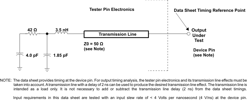 Figure 5-1 3.3-V Test Load Circuit for AC Timing Measurements
The load capacitance value stated is only for characterization and measurement of AC timing signals. This load capacitance value does not indicate the maximum load the device is capable of driving.
5.7.1.1 1.8-V, 2.75-V, and 3.3-V Signal Transition Levels
All rise and fall transition timing parameters are referenced to VIL MAX and VIH MIN for input clocks, VOL MAX and VOH MIN for output clocks.
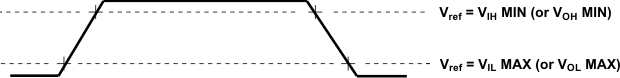 Figure 5-2 Rise and Fall Transition Time Voltage Reference Levels
5.7.1.2 3.3-V Signal Transition Rates
All timings are tested with an input edge rate of 4 volts per nanosecond (4 V/ns).
5.7.1.3 Timing Parameters and Board Routing Analysis
The timing parameter values specified in this data manual do not include delays by board routing. As a good board design practice, such delays must always be taken into account. Timing values may be adjusted by increasing and decreasing such delays. TI recommends utilizing the available I/O buffer information specification (IBIS) models to analyze the timing characteristics correctly. To properly use IBIS models to attain accurate timing analysis for a given system, see the Using IBIS Models for Timing Analysis application report [literature number SPRA839]. If needed, external logic hardware such as buffers may be used to compensate any timing differences.
5.7.2 Power Supplies
5.7.2.1 Power Considerations
The device provides several means of managing power consumption.
To minimize power consumption, the device divides its circuits into nine main isolated supply domains:
- LDOI (LDOs and Bandgap Power Supply)
- Analog POR, SAR, and PLL (VDDA_ANA and VDDA_PLL)
- RTC Core (CVDDRTC) — Note: CVDDRTC must always be powered by an external power source. None of the on-chip LDOs can be used to power CVDDRTC.
- Digital Core (CVDD)
- USB Core (USB_VDD1P3 and USB_VDDA1P3)
- USB PHY and USB PLL (USB_VDDOSC, USB_VDDA3P3, and USB_VDDPLL)
- EMIF I/O (DVDDEMIF)
- RTC I/O (DVDDRTC)
- Rest of the I/O (DVDDIO)
5.7.2.1.1 LDO Configuration
The device includes three Low-Dropout Regulators (LDOs) which can be used to regulate the power supplies of the SAR ADC and Power Management (ANA_LDO), Digital Core (DSP_LDO), and USB Core (USB_LDO).
These LDOs are controlled by a combination of pin configuration and register settings. For more detailed information see the following sections.
5.7.2.1.1.1 LDO Inputs
The LDOI pins (B12, F13, F14) provide power to the internal Analog LDO, DSP LDO, USB LDO, the bandgap reference generator, and some I/O input pins, and can range from 1.8 V to 3.6 V. The bandgap provides accurate voltage and current references to the POR, LDOs, PLL, and SAR; therefore, for proper device operation, power must always be applied to the LDOI pins even if the LDO outputs are not used.
5.7.2.1.1.2 LDO Outputs
The ANA_LDOO pin (A12) is the output of the internal ANA_LDO and can provide regulated 1.3 V power of up to 4 mA. The ANA_LDOO pin is intended to be connected, on the board, to the VDDA_ANA pin to provide a regulated 1.3 V to the 10-bit SAR ADC and Power Management Circuits. VDDA_ANA may be powered by this LDO output, which is recommended, to take advantage of the device's power management techniques, or by an external power supply. The ANA_LDO cannot be disabled individually (see Section 5.7.2.1.1.2.1, LDO Control).
The DSP_LDOO pin (E10) is the output of the internal DSP_LDO and provides software-selectable regulated 1.3 V or regulated 1.05 V power of up to 250 mA. The DSP_LDOO pin is intended to be connected, on the board, to the CVDD pins. In this configuration, the DSP_LDO_EN pin should be tied to the board VSS, thus enabling the DSP_LDO.
Optionally, the CVDD pins may be powered by an external power supply. In this configuration the DSP_LDO_EN pin should be tied (high) to LDOI, disabling DSP_LDO.
The DSP_LDO_EN also affects how reset is generated to the chip (for more details, see the DSP_LDO_EN pin description in Table 4-17, Regulators and Power Management Signal Descriptions). When the DSP_LDO is disabled, its output pin is in a high-impedance state.
The LDOs cannot supply power to CVDDRTC, which requires an external power source because CVDDRTC must always be on for proper operation.
NOTE
DSP_LDO can only provide a regulated 1.05 V or 1.3 V. When the DSP Core (CVDD) requires 1.4 V, an external supply is required to supply 1.4 V to the DSP Core (CVDD) and the DSP_LDO_EN pin should be tied to LDOI.
The USB_LDOO pin (F12) is the output of the internal USB_LDO and provides regulated 1.3 V, software-switchable (on and off) power of up to 25 mA. The USB_LDOO pin is intended to be connected, on the board, to the USB_VDD1P3 and USB_VDDA1P3 pins to provide power to portions of the USB. Optionally, the USB_VDD1P3 and USB_VDDA1P3 may be powered by an external power supply and the USB_LDO can be left disabled. When the USB_LDO is disabled, its output pin is in a high-impedance state.
5.7.2.1.1.2.1 LDO Control
All three LDOs can be simultaneously disabled via software by writing to either the BG_PD bit or the LDO_PD bit in the RTCPMGT register (see Figure 5-3). When the LDOs are disabled via this mechanism, the only way to re-enable them is by cycling power to the CVDDRTC pin.
ANA_LDO: The ANA_LDO is only disabled by the BG_PD and the LDO_PD mechanism described above. Otherwise, it is always enabled.
DSP_LDO: The DSP_LDO can be statically disabled by the DSP_LDO_EN pin as described in Section 5.7.2.1.1.2, LDO Outputs. The DSP_LDO can also be dynamically enabled and disabled via the BG_PD and the LDO_PD mechanism described above. The DSP_LDO can change its output voltage dynamically by software via the DSP_LDO_V bit in the LDOCNTL register (see Figure 5-4). The DSP_LDO output voltage is set to 1.3 V at reset.
USB_LDO: The reset state of the USB_LDO is dependent on the setting of CLK_SEL pin. If CLK_SEL is high, the USB_LDO is disabled but can be independently and dynamically enabled or disabled by software via the USB_LDO_EN bit in the LDOCNTL register (see Figure 5-4). If CLK_SEL is low, the USB LDO is enabled at reset and can never be disabled. This is to ensure the USB oscillator has power when it is the source of the system clock.
Table 5-3 shows the ON and OFF control of each LDO and its register control bit configurations.
| 15 | 14 | 13 | 12 | 11 | 10 | 9 | 8 |
| Reserved | |||||||
| R-0 | |||||||
| 7 | 6 | 5 | 4 | 3 | 2 | 1 | 0 |
| Reserved | WU_DOUT | WU_DIR | BG_PD | LDO_PD | RTCCLKOUTEN | ||
| R/W-1 | R/W-0 | R/W-0 | R/W-0 | R/W-0 | |||
| LEGEND: R/W = Read/Write; R = Read only; -n = value after reset |
Table 5-1 RTCPMGT Register Bit Descriptions
| Bit | Name | Description |
|---|---|---|
| 15:5 | Reserved | Reserved. Read-only, writes have no effect. |
| 4 | WU_DOUT | Wakeup output, active low, open-drain. 0 = WAKEUP pin driven low. 1 = WAKEUP pin is in high-impedance (Hi-Z). |
| 3 | WU_DIR | Wakeup pin direction control. 0 = WAKEUP pin configured as a input. 1 = WAKEUP pin configured as a output. Note: When the WAKEUP pin is configured as an input, it is active high. When the WAKEUP pin is configured as an output, is an open-drain that is active low and should be externally pulled-up via a 10-kΩ resistor to DVDDRTC. WU_DIR must be configured as an input to allow the WAKEUP pin to wake the device up from idle modes. |
| 2 | BG_PD | Bandgap, on-chip LDOs, and the analog POR power down bit. This bit shuts down the on-chip LDOs (ANA_LDO, DSP_LDO, and USB_LDO), the Analog POR, and Bandgap reference. BG_PD and LDO_PD are only intended to be used when the internal LDOs supply power to the chip. If the internal LDOs are bypassed and not used then the BG_PD and LDO_PD power-down mechanisms should not be used. After this bit is asserted, the on-chip LDOs, Analog POR, and the Bandgap reference can be re-enabled by the WAKEUP pin (high) or the RTC alarm interrupt. The Bandgap circuit will take about 100 msec to charge the external 0.1 uF capacitor via the internal 326-kΩ resistor. 0 = On-chip LDOs, Analog POR, and Bandgap reference are enabled. 1 = On-chip LDOs, Analog POR, and Bandgap reference are disabled (shutdown). |
| 1 | LDO_PD | On-chip LDOs and Analog POR power down bit. This bit shuts down the on-chip LDOs (ANA_LDO, DSP_LDO, and USB_LDO) and the Analog POR. BG_PD and LDO_PD are only intended to be used when the internal LDOs supply power to the chip. If the internal LDOs are bypassed and not used then the BG_PD and LDO_PD power-down mechanisms should not be used. After this bit is asserted, the on-chip LDOs and Analog POR can be re-enabled by the WAKEUP pin (high) or the RTC alarm interrupt. This bit keeps the Bandgap reference turned on to allow a faster wake-up time with the expense power consumption of the Bandgap reference. 0 = On-chip LDOs and Analog POR are enabled. 1 = On-chip LDOs and Analog POR are disabled (shutdown). |
| 0 | RTCCLKOUTEN | Clockout output enable bit. 0 = Clock output disabled. 1 = Clock output enabled. |
| 15 | 14 | 13 | 12 | 11 | 10 | 9 | 8 |
| Reserved | |||||||
| R-0 | |||||||
| 7 | 6 | 5 | 4 | 3 | 2 | 1 | 0 |
| Reserved | DSP_LDO_V | USB_LDO_EN | |||||
| R-0 | R/W-0 | R/W-CLK_SEL | |||||
| LEGEND: R/W = Read/Write; R = Read only; -n = value after reset |
Table 5-2 LDOCNTL Register Bit Descriptions
| Bit | Name | Description |
|---|---|---|
| 15:2 | Reserved | Reserved. Read-only, writes have no effect. |
| 1 | DSP_LDO_V | DSP_LDO voltage select bit. 0 = DSP_LDOO is regulated to 1.3 V. 1 = DSP_LDOO is regulated to 1.05 V. |
| 0 | USB_LDO_EN | USB_LDO enable bit. The reset state of this bit is dependent on the setting of CLK_SEL pin at reset. If CLK_SEL is high, the USB_LDO is disabled (USB_LEO_EN = 0). If CLK_SEL is low, the USB LDO is enabled (USB_LDO_EN=1). 0 = USB_LDO output is disabled. USB_LDOO pin is placed in high-impedance (Hi-Z) state. 1 = USB_LDO output is enabled. USB_LDOO is regulated to 1.3 V. Note: When CLK_SEL = 0, this bit will not be able to be set to 0 and the USB_LDO will stay enabled. |
Table 5-3 LDO Controls Matrix
| RTCPMGT Register (0x1930) |
LDOCNTL Register (0x7004) |
DSP_LDO_EN (Pin D12) |
CLK_SEL (Pin C7) |
ANA_LDO | DSP_LDO | USB_LDO | |
|---|---|---|---|---|---|---|---|
| BG_PD Bit | LDO_PD Bit | USB_LDO_EN Bit | |||||
| 1 | Don't Care | Don't Care | Don't Care | 0 | OFF | OFF | ON |
| Don't Care | 1 | Don't Care | Don't Care | 0 | OFF | OFF | ON |
| 0 | 0 | Don't Care | Low | 0 | ON | ON | ON |
| 0 | 0 | Don't Care | High | 0 | ON | OFF | ON |
| 1 | Don't Care | Don't Care | Don't Care | 1 | OFF | OFF | OFF |
| Don't Care | 1 | Don't Care | Don't Care | 1 | OFF | OFF | OFF |
| 0 | 0 | 0 | Low | 1 | ON | ON | OFF |
| 0 | 0 | 0 | High | 1 | ON | OFF | OFF |
| 0 | 0 | 1 | Low | 1 | ON | ON | ON |
| 0 | 0 | 1 | High | 1 | ON | OFF | ON |
5.7.2.2 Power-Supply Sequencing
The device includes four core voltage-level supplies (CVDD, CVDDRTC, USB_VDD1P3, USB_VDDA1P3), and several I/O supplies including—DVDDIO, DVDDEMIF, DVDDRTC, USB_VDDOSC, and USB_VDDA3P3.
Some TI power-supply devices include features that facilitate power sequencing—for example, Auto-Track and Slow-Start and Enable features. For more information regarding TI's power management products and suggested devices to power TI DSPs, visit www.ti.com/processorpower.
The device does not require a specific power-up sequence. However, if the DSP_LDO is disabled (DSP_LDO_EN = high) and an external regulator supplies power to the CPU Core (CVDD), the external reset signal (RESET) must be held asserted until all of the supply voltages reach their valid operating ranges.
Note: the external reset signal on the RESET pin must be held low until all of the power supplies reach their operating voltage conditions.
The I/O design allows either the core supplies (CVDD, CVDDRTC, USB_VDD1P3, USB_VDDA1P3) or the I/O supplies (DVDDIO, DVDDEMIF, DVDDRTC, USB_VDDOSC, and USB_VDDA3P3) to be powered up for an indefinite period of time while the other supply is not powered if the following constraints are met:
- All maximum ratings and recommended operating conditions are satisfied.
- All warnings about exposure to maximum rated and recommended conditions, particularly junction temperature are satisfied. These apply to power transitions as well as normal operation.
- Bus contention while core supplies are powered must be limited to 100 hours over the projected lifetime of the device.
- Bus contention while core supplies are powered down does not violate the absolute maximum ratings.
If the USB subsystem is used, the subsystem must be powered up in the following sequence:
- USB_VDDA1P3 and USB_VDD1P3
- USB_VDDA3P3
- USB_VBUS
If the USB subsystem is not used, the following can be powered off:
- USB Core
- USB_VDD1P3
- USB_VDDA1P3
- USB PHY and I/O Level Supplies
- USB_VDDOSC
- USB_VDDA3P3
- USB_VDDPLL
A supply bus is powered up when the voltage is within the recommended operating range. The supply bus is powered down when the voltage is below that range, either stable or while in transition.
5.7.2.3 Digital I/O Behavior When Core Power (CVDD) is Down
With some exceptions (listed below), all digital I/O pins on the device have special features to allow powering down of the Digital Core Domain (CVDD) without causing I/O contentions or floating inputs at the pins (see Figure 5-5). The device asserts the internal signal called HHV high when power has been removed from the Digital Core Domain (CVDD). Asserting the internal HHV signal causes the following conditions to occur in any order:
- All output pin strong drivers to go to the high-impedance (Hi-Z) state
- Weak bus holders to be enabled to hold the pin at a valid high or low
- The internal pullups or pulldowns (IPUs and IPDs) on the I/O pins will be disabled
The exception pins that do not have this special feature are:
- Pins driven by the CVDDRTC Power Domain [This power domain is "Always On"; therefore, the pins driven by CVDDRTCdo not need these special features]:
- RTC_XI, RTC_XO, RTC_CLKOUT, and WAKEUP
- USB Pins:
- USB_DP, USB_DM, USB_R1, USB_VBUS, USB_MXI, and USB_MXO
- Pins for the Analog Block:
- GPAIN[3:0], DSP_LDO_EN, and BG_CAP
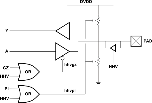 Figure 5-5 Bus Holder I/O Circuit
NOTE
Figure 5-5 shows both a pullup and pulldown but pins only have one, not both.
PI = Pullup and Pulldown Inhibit
GZ = Output Enable (active low)
HHV = Described in Section 5.7.2.3
5.7.2.4 Power-Supply Design Considerations
Core and I/O supply voltage regulators should be located close to the DSP (or DSP array) to minimize inductance and resistance in the power delivery path. Additionally, when designing for high-performance applications utilizing the device, the PC board should include separate power planes for core, I/O, VDDA_ANA and VDDA_PLL (which can share the same PCB power plane), and ground; all bypassed with high–quality low–ESL and ESR capacitors.
5.7.2.5 Power-Supply Decoupling
In order to properly decouple the supply planes from system noise, place capacitors (caps) as close as possible to the device. These caps need to be no more than 1.25 cm maximum distance from the device power pins to be effective. Physically smaller caps, such as 0402, are better but need to be evaluated from a yield and manufacturing point-of-view. Parasitic inductance limits the effectiveness of the decoupling capacitors, therefore physically smaller capacitors should be used while maintaining the largest available capacitance value.
Larger caps for each supply can be placed further away for bulk decoupling. Large bulk caps (on the order of 10 µF) should be furthest away, but still as close as possible. Large caps for each supply should be placed outside of the BGA footprint.
As with the selection of any component, verification of capacitor availability over the product's production lifetime should be considered.
The recommended decoupling capacitance for the DSP core supplies should be 1 µF in parallel with 0.01-µF capacitor per supply pin.
5.7.2.6 LDO Input Decoupling
The LDO inputs should follow the same decoupling guidelines as other power-supply pins above.
5.7.2.7 LDO Output Decoupling
The LDO circuits implement a voltage feedback control system which has been designed to optimize gain and stability tradeoffs. As such, there are design assumptions for the amount of capacitance on the LDO outputs. For proper device operation, the following external decoupling capacitors should be used when the on-chip LDOs are enabled:
- ANA_LDOO– 1µF
- DSP_LDOO – 5µF ~ 10µF
- USB_LDOO – 1µF ~ 2µF
5.7.3 Reset
The device has two main types of reset: hardware reset and software reset.
Hardware reset is responsible for initializing all key states of the device. The hardware reset occurs whenever the RESET pin is asserted or when the internal power-on-reset (POR) circuit deasserts an internal signal called POWERGOOD. The device's internal POR is a voltage comparator that monitors the DSP_LDOO pin voltage and generates the internal POWERGOOD signal when the DSP_LDO is enabled externally by the DSP_LDO_EN pin. POWERGOOD is asserted when the DSP_LDOO voltage is above a minimum threshold voltage provided by the bandgap. When the DSP_LDO is disabled (DSP_LDO_EN is high), the internal voltage comparator becomes inactive, and the POWERGOOD signal logic level is immediately set high. The RESET pin and the POWERGOOD signal are internally combined with a logical AND gate to produce an (active low) hardware reset (see Figure 5-6, Power-On Reset Timing Requirements and Figure 5-7, Reset Timing Requirements).
There are two types of software reset: the CPU's software reset instruction and the software control of the peripheral reset signals. For more information on the CPU's software reset instruction, see the C55x CPU 3.0 CPU Reference Guide [literature number: SWPU073]. In all the device documentation, all references to "reset" refer to hardware reset. Any references to software reset will explicitly state software reset.
The device RTC has one additional type of reset, a power-on-reset (POR) for the registers in the RTC core. This POR monitors the voltage of CVDDRTC and resets the RTC registers when power is first applied to the RTC core.
5.7.3.1 Power-On Reset (POR) Circuits
The device includes two power-on reset (POR) circuits, one for the RTC (RTC POR) and another for the rest of the chip (MAIN POR).
5.7.3.1.1 RTC Power-On Reset (POR)
The RTC POR ensures that the flip-flops in the CVDDRTC power domain have an initial state upon powerup. In particular, the RTCNOPWR register is reset by this POR and is used to indicate that the RTC time registers need to be initialized with the current time and date when power is first applied.
5.7.3.1.2 Main Power-On Reset (POR)
The device includes an analog power-on reset (POR) circuit that keeps the DSP in reset until specific voltages have reached predetermined levels. When the DSP_LDO is enabled externally by the DSP_LDO_EN pin, the output of the POR circuit, POWERGOOD, is held low until the following conditions are satisfied:
- LDOI is powered and the bandgap is active for at least approximately 8 ms
- VDD_ANA is powered for at least approximately 4 ms
- DSP_LDOO is above a threshold of approximately 950 mV (see the following Note:)
Note: The POR comparator has hysteresis, so the threshold voltage becomes approximately 850 mV after POWERGOOD signal is set high.
Once these conditions are met, the internal POWERGOOD signal is set high. The POWERGOOD signal is internally combined with the RESET pin signal, via an AND-gate, to produce the DSP subsystem's global reset. This global reset is the hardware reset for the whole chip, except the RTC. When the global reset is deasserted (high), the boot sequence starts. For more detailed information on the boot sequence, see Section 6.4.1, Boot Sequence.
When the DSP_LDO is disabled (DSP_LDO_EN pin = 1), the voltage monitoring on the DSP_LDOO pin is de-activated and the POWERGOOD signal is immediately set high. The RESET pin will be the sole source of hardware reset.
5.7.3.1.3 Reset Pin (RESET)
The device can receive an external reset signal on the RESET pin. As specified above in Section 5.7.3.1.2, Main Power-On Reset, the RESET pin is combined with the internal POWERGOOD signal, that is generated by the MAIN POR, via an AND-gate. The output of the AND gate provides the hardware reset to the chip. The RESET pin may be tied high and the MAIN POR can provide the hardware reset in case DSP_LDO is enabled (DSP_LDO_EN = 0), but an external hardware reset must be provided via the RESET pin when the DSP_LDO is disabled (DSP_LDO_EN = 1).
Once the hardware reset is applied, the system clock generator is enabled and the DSP starts the boot sequence. For more information on the boot sequence, see Section 6.4.1, Boot Sequence.
5.7.3.2 Pin Behavior at Reset
All pins are in Hi-Z state when RESET is applied, and pins are held in Hi-Z state for the first two clock cycles after RESET is de-asserted (set to high).
During normal operation, pins are controlled by the respective peripheral selected in the External Bus Selection Register (EBSR) register. During power-on reset and reset, the behavior of the output pins changes and is categorized as follows:
| Z, High Group:EM_CS2, EM_CS3, EM_CS4, EM_CS5, EM_DQM0/UHPI_HBE0, EM_DQM1/UHPI_HBE1, EM_OE, EM_SDCAS/UHPI_HCS, EM_SDRAS/UHPI_HAS, EM_WE, XF | |
| Z, Low Group: SPI_CLK/UHPI_HINT, I2S2_DX/UHPI_HD[11]/GP[27]/SPI_TX, EM_R/W, MMC0_CLK/I2S0_CLK/GP[0]/McBSP_CLKX, MMC1_CLK/McSPI_CLK/GP[6], EM_SDCLK | |
| Z Group: EM_D[0:15], GP[21:26]/EM_A[15:20], GP[12:17]/UHPI_HD[2:7], EM_WAIT2, EM_WAIT3, EM_WAIT4, EM_WAIT5, EMU0, EMU1, SCL, SDA, TDO, USB_MXO, WAKEUP, RTC_CLKOUT | |
| I2S2_CLK/UHPI_HD[8]/GP[18]/SPI_CLK, I2S2_FS/UHPI_HD[9]/GP[19]/SPI_CS0, I2S2_RX/UHPI_HD[10]/GP[20]/SPI_RX | |
| MMC0_CMD/I2S0_FS/GP[1]/McBSP_FSX, MMC0_D0/I2S0_DX/GP[2]/McBSP_DX, MMC0_D1/I2S0_RX/GP[3]/McBSP_DR, MMC0_D2/GP[4]/McBSP_FSR, MMC0_D3/GP[5]/McBSP_CLKR_CLKS | |
| MMC1_CMD/McSPI_CS0/GP[7], MMC1_D0/McSPI_SIMO/GP[8], MMC1_D1/McSPI_SOMI/GP[9], MMC1_D2/McSPI_CS1/GP[10], MMC1_D3/McSPI_CS2/GP[11] | |
| UART_CTS/UHPI_HD[13]/GP[29]/I2S3_FS, UART_RXD/UHPI_HD[14]/GP[30]/I2S3_RX, SPI_TX/UHPI_HD[1], SPI_RX/UHPI_HD[0] | |
| Z, CLKOUT Group: CLKOUT | |
| Z Group - Analog: GPAIN0, GPAIN1, GPAIN2, GPAIN3 | |
| Z, SYNCH 0→1 Group: EM_SDCKE/UHPI_HHWIL | |
| Z, SYNCH 1→0 Group:EM_CS0/UHPI_HDS1, EM_CS1/UHPI_HDS2 | |
| Z, SYNCH22 0→1 Group: SPI_CS0/UHPI_HCNTL0, SPI_CS1/UHPI_HCNTL1, SPI_CS2/UHPI_HR_NW, SPI_CS3/UHPI_HRDY | |
| Z, SYNCH X→1 Group:EM_BA[0], EM_BA[1], UART_RTS/UHPI_HD[12]/GP[28]/I2S3_CLK, UART_TXD/UHPI_HD[15]/GP[31]/I2S3_DX | |
| Z, SYNCH X→0 Group: EM_A[0:10], EM_A[11]/(ALE), EM_A[12]/(CLE), EM_A[13], EM_A[14] |
5.7.3.3 Reset Electrical Data and Timing
Table 5-4 Timing Requirements for Reset(1) (see Figure 5-6 and Figure 5-7)
| NO. | CVDD = 1.05 V | CVDD = 1.3/1.4 V | UNIT | ||||
|---|---|---|---|---|---|---|---|
| MIN | MAX | MIN | MAX | ||||
| 1 | tw(RSTL) | Pulse duration, RESET low | 3P | 3P | ns | ||
For a description of IDLE3 mode, see the System chapter in the TMS320C5517 Digital Signal Processor Technical Reference Manual [literature number SPRUH16].
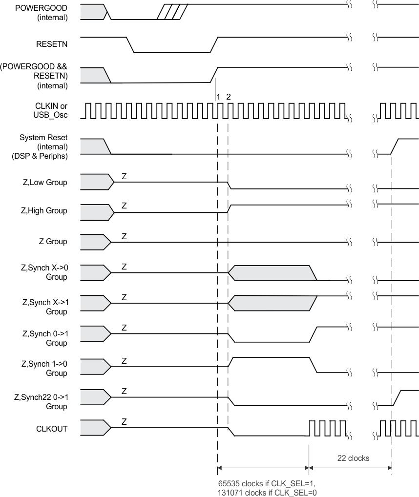 Figure 5-6 Reset Timing When DSP_LDO_EN = 0
 Figure 5-7 Reset Timing When DSP_LDO_EN = 1
5.7.3.4 Configurations at Reset
Some device configurations are determined at reset. The following subsections give more details.
5.7.3.4.1 Device and Peripheral Configurations at Device Reset
Table 5-5 summarizes the device boot and configuration pins that are required to be statically tied high, tied low, or left unconnected during device operation. For proper device operation, a device reset should be initiated after changing any of these pin functions.
Table 5-5 Default Functions Affected by Device Configuration Pins
| CONFIGURATION PINS | SIGNAL NO. | IPU and IPD | FUNCTIONAL DESCRIPTION |
|---|---|---|---|
| DSP_LDO_EN | D12 | – | DSP_LDO enable input. This signal is not intended to be dynamically switched. 0 = DSP_LDO is enabled. The internal DSP LDO is enabled to regulate power on the DSP_LDOO pin at either 1.3 V or 1.05 V according to the LDO_DSP_V bit in the LDOCNTL register, see Figure 5-4). At power-on-reset, the internal POR monitors the DSP_LDOO pin voltage and generates the internal POWERGOOD signal when the DSP_LDO voltage is above a minimum threshold voltage. The internal device reset is generated by the AND of POWERGOOD and the RESET pin. 1 = DSP_LDO is disabled and the DSP_LDOO pin is in high-impedance (Hi-Z). The internal voltage monitoring on the DSP_LDOO is bypassed and the internal POWERGOOD signal is immediately set high. The RESET pin (D6) will act as the sole reset source for the device. If an external power supply is used to provide power to CVDD, then DSP_LDO_EN should be tied to LDOI, DSP_LDOO should be left unconnected, and the RESET pin must be asserted appropriately for device initialization after powerup. Note: to pullup this pin, connect it to the same supply as LDOI pins. |
| CLK_SEL | C7 | – | Clock input select. 0 = The on-chip USB oscillator is enabled and drives the system clock generator. Also, the USB LDOO is enabled at reset (USB_LDO_EN=1). In this configuration, CLKIN must be tied to GND. 1 = CLKIN drives the system clock generator. The on-chip USB oscillator and USB_LDO are disabled at reset (USB_LDO_EN=0) but can be enabled by software This pin is not allowed to change during device operation; it must be tied to DVDDIO or GND at the board. |
For proper device operation, external pullup and pulldown resistors may be required on these device configuration pins. For discussion on situations where external pullup and pulldown resistors are required, see Section 5.7.20.1.1, Pullup and Pulldown Resistors.
This device also has RESERVED pins that need to be configured correctly for proper device operation (statically tied high, tied low, or left unconnected at all times). For more details on these pins, see Table 4-24, Reserved and No Connects Signal Descriptions.
5.7.3.4.2 BootMode Implementation and Requirements
The EM_A[20:15]/GP[26:21] pins are used to latch the bootmode, as defined in Table 6-34. These pins are defined as GPIO function at reset and they are in input state. Therefore these pins can be driven to the desired bootmode terminations at reset. Approximately 10 system cycles after the rising edge of the RESET pin, the state on these pins will be latched into registers readable by the DSP at IO-space address 0x1C5A.
As the bootloader code starts executing, it reads the latched value in the bootmode register and uses that value to determine from which peripheral or method to boot. In any case where the ASYNC modes (except for NAND) are used as the source data for bootloading (for example, bootload from external NOR flash to internal memory), the bootloader routine in ROM will change the EM_A[20:15] or GP[26:21] pins from GPIO mode to EMIF mode by writing to the EBSR (0x1C00). When this occurs, no signal contentions must be on the EM_A[20:15] or GP[26:21] pins. Passive static terminations by external pullup or pulldown resistors should also be considered.
Note: Bootloading directly to external peripherals on the EMIF is not supported because the EMIF clock is turned off before jumping to bootloaded code.
The bootloader must enable the EMIF function on these pins in order to increase the address reach from 15-bits (EM_A[14:0] 32 kW) to the full 21-bits (EM_A[20:0] 2 MW). The bootloader does not have to enable the EMIF mode on the EM_A[20:15] or GP[26:21] pins for the following external memory types:
NAND: Uses the EM_D[15:0] pins for both address and data and command signaling.
SDRAM: Uses column and row addressing using no more than 11 bits of EM_A pins
The following image contains two BootMode termination scenarios. Other options are also possible.
 Figure 5-8 BootMode Termination Scenarios
5.7.3.5 Configurations After Reset
The following sections provide details on configuring the device after reset. Multiplexed pin functions are selected by software after reset. For more details on multiplexed pin function control, see Section 4.3, Pin Multiplexing.
5.7.3.5.1 External Bus Selection Register (EBSR)
The External Bus Selection Register (EBSR) determines the mapping of the UHPI, I2S2, I2S3, UART, SPI, McBSP, McSPI, and GPIO signals to 28 signals of the external parallel port pins. The EBSR also determines the mapping of the I2S, McBSP, McSPI, GPIO, or MMC and SD ports to serial port 0 pins and serial port 1 pins. The EBSR register is located at IO-space 0x1C00. Once the bit fields of this register are changed, the routing of the signals takes place on the next CPU clock cycle.
In addition, the EBSR controls the function of the upper bits of the EMIF address bus. Pins EM_A[20:15] or GP[26:21] can be individually configured as GPIO pins through the Axx_MODE bits. When Axx_MODE = 1, the EM_A[xx] pin functions as a GPIO pin. When Axx_MODE = 0, the EM_A[xx] pin has EMIF address output functionality.
Before modifying the values of the external bus selection register, you must clock gate all affected peripherals through the Peripheral Clock Gating Control Register. After the external bus selection register has been modified, you must reset the peripherals before using them through the Peripheral Software Reset Counter Register.
| 15 | 14 | 13 | 12 | 11 | 10 | 9 | 8 |
| McBSP_CLKS Selection | PPMODE | SP1MODE | SP0MODE | ||||
| R/W-0 | R/W-001 | R/W-00 | R/W-00 | ||||
| 7 | 6 | 5 | 4 | 3 | 2 | 1 | 0 |
| Reserved | A20_MODE | A19_MODE | A18_MODE | A17_MODE | A16_MODE | A15_MODE | |
| R-0 | R/W-1 | R/W-1 | R/W-1 | R/W-1 | R/W-1 | R/W-1 | |
| LEGEND: R/W = Read/Write; R = Read only; -n = value after reset |
Table 5-6 EBSR Register Field Descriptions
| Bit | Field | Description |
|---|---|---|
| McBSP_CLKS Selection | ||
| 15 | McBSP_CLKS Selection | 0 = McBSP_CLKR signal is routed to MMC0_D3/GP[5]/McBSPCLKR_CLKS (L11) when SP0MODE=3 |
| 1 = McBSP_CLKS signal is routed to MMC0_D3/GP[5]/McBSPCLKR_CLKS (L11) when SP0MODE=3 | ||
| 14:12 | PPMODE | Parallel Port Mode Control Bits. These bits control the pin multiplexing of the UHPI, SPI, UART, I2S2, I2S3, and GP[31:27, 20:12] pins on the parallel port. For more details, see Table 4-20. 000 = Mode 0 (16-bit UHPI bus). All 28 signals of the UHPI bus module are routed to the 28 external signals of the parallel port. Note: SDRAM control signals are multiplexed with UHPI bus control signals. In this mode, UHPI bus signals are routed to the control ports, so SDRAM cannot be accessible. 001 = Mode 1 (SPI, GPIO, UART, I2S2, and SDRAM). 7 signals of the SPI module, 6 GPIO signals, 4 signals of the UART module, 4 signals of the I2S2 module, and 7 SDRAM control signals are routed to the 28 external signals of the parallel port. 010 = Mode 2 (GPIO and SDRAM). 8 GPIO and 7 SDRAM control signals are routed to the 28 external signals of the parallel port. 011 = Mode 3 (SPI, I2S3, and SDRAM). 4 signals of the SPI module, 4 signals of the I2S3 module, and 7 SDRAM control signals are routed to the 28 external signals of the parallel port. 100 = Mode 4 (I2S2, UART, and SDRAM). 4 signals of the I2S2 module, 4 signals of the UART module, and 7 SDRAM control signals are routed to the 28 external signals of the parallel port. 101 = Mode 5 (SPI, UART, and SDRAM). 4 signals of the SPI module, 4 signals of the UART module, and 7 SDRAM control signals are routed to the 28 external signals of the parallel port. 110 = Mode 6 (SPI, I2S2, I2S3, GPIO, and SDRAM). 7 signals of the SPI module, 4 signals of the I2S2 module, 4 signals of the I2S3 module, 6 GPIO, and 7 SDRAM control signals are routed to the 28 external signals of the parallel port. 111 = Reserved. |
| 11:10 | SP1MODE | Serial Port 1 Mode Control Bits. The bits control the pin multiplexing of the MMC1, McSPI, and GPIO pins on serial port 1. For more details, see Table 4-21. 00 = Mode 0 (MMC1 and SD1). All 6 signals of the MMC1 and SD1 module are routed to the 6 external signals of the serial port 1. 01 = Mode 1 (McSPI). 6 signals of the McSPI module signals are routed to the 6 external signals of the serial port 1. 10 = Mode 2 (GP[11:6]). 6 GPIO signals (GP[11:6]) are routed to the 6 external signals of the serial port 1. 11 = Reserved. |
| 9:8 | SP0MODE | Serial Port 0 Mode Control Bits. The bits control the pin multiplexing of the MMC0, I2S0, McBSP, and GPIO pins on serial port 0. For more details, see Section 4.3.3. 00 = Mode 0 (MMC0 and SD0). All 6 signals of the MMC0 and SD0 module are routed to the 6 external signals of the serial port 0. 01 = Mode 1 (I2S0 and GP[5:4]). 4 signals of the I2S0 module and 2 GP[5:4] signals are routed to the 6 external signals of the serial port 0. 10 = Mode 2 (GP[5:0]). 6 GPIO signals (GP[5:0]) are routed to the 6 external signals of the serial port 0. 11 = Mode 3 (McBSP). 6 signals of the McBSP module are routed to the 6 external signal port 0. |
| 7-6 | Reserved | Reserved. Read-only, writes have no effect. |
| 5 | A20_MODE | A20 Pin Mode Bit. This bit controls the pin multiplexing of the EMIF address 20 (EM_A[20]) and general-purpose input/output pin 26 (GP[26]) pin functions. 0 = Pin function is EMIF address pin 20 (EM_A[20]). 1 = Pin function is general-purpose input/output pin 26 (GP[26]). This is the default mode at reset and the pin is configured as an Input. Approximately 10 cycles after the rising edge of RESET, the state on this pin is latched into the BootMode register to specify the boot method. |
| 4 | A19_MODE | A19 Pin Mode Bit. This bit controls the pin multiplexing of the EMIF address 19 (EM_A[19]) and general-purpose input/output pin 25 (GP[25]) pin functions. 0 = Pin function is EMIF address pin 19 (EM_A[19]). 1 = Pin function is general-purpose input/output pin 25 (GP[25]). This is the default mode at reset and the pin is configured as an Input. Approximately 10 cycles after the rising edge of RESET, the state on this pin is latched into the BootMode register to specify the boot method. |
| 3 | A18_MODE | A18 Pin Mode Bit. This bit controls the pin multiplexing of the EMIF address 18 (EM_A[18]) and general-purpose input/output pin 24 (GP[24]) pin functions. 0 = Pin function is EMIF address pin 18 (EM_A[18]). 1 = Pin function is general-purpose input/output pin 24 (GP[24]). This is the default mode at reset and the pin is configured as an Input. Approximately 10 cycles after the rising edge of RESET, the state on this pin is latched into the BootMode register to specify the boot method. |
| 2 | A17_MODE | A17 Pin Mode Bit. This bit controls the pin multiplexing of the EMIF address 17 (EM_A[17]) and general-purpose input/output pin 23 (GP[23]) pin functions. For more details, see Table 4-22, MMC0, I2S0, McBSP, and GP[5:0] Pin Multiplexing. 0 = Pin function is EMIF address pin 17 (EM_A[17]). 1 = Pin function is general-purpose input/output pin 23 (GP[23]). This is the default mode at reset and the pin is configured as an Input. Approximately 10 cycles after the rising edge of RESET, the state on this pin is latched into the BootMode register to specify the boot method. |
| 1 | A16_MODE | A16 Pin Mode Bit. This bit controls the pin multiplexing of the EMIF address 16 (EM_A[16]) and general-purpose input/output pin 22 (GP[22]) pin functions. For more details, see Table 4-22, MMC0, I2S0, McBSP, and GP[5:0] Pin Multiplexing. 0 = Pin function is EMIF address pin 16 (EM_A[16]). 1 = Pin function is general-purpose input/output pin 22 (GP[22]). This is the default mode at reset and the pin is configured as an Input. Approximately 10 cycles after the rising edge of RESET, the state on this pin is latched into the BootMode register to specify the boot method. |
| 0 | A15_MODE | A15 Pin Mode Bit. This bit controls the pin multiplexing of the EMIF address 15 (EM_A[15]) and general-purpose input/output pin 21 (GP[21]) pin functions. For more details, see Table 4-22, MMC0, I2S0, McBSP, and GP[5:0] Pin Multiplexing. 0 = Pin function is EMIF address pin 15 (EM_A[15]). 1 = Pin function is general-purpose input/output pin 21 (GP[21]). This is the default mode at reset and the pin is configured as an Input. Approximately 10 cycles after the rising edge of RESET, the state on this pin is latched into the BootMode register to specify the boot method. |
5.7.3.5.2 LDO Control Register [7004h]
When the DSP_LDO is enabled by the DSP_LDO_EN pin being tied low, the DSP_LDOO voltage is set by the DSP_LDO_V bit in this register. The reset state of this bit causes the DSP_LDOO output to be set to 1.3 V at boot. The DSP_LDOO voltage can be programmed to be either 1.05 V or 1.3 V via the DSP_LDO_V bit (bit 1) in the LDO Control Register (LDOCNTL).
At reset, the USB_LDO state is dependent on the CLK_SEL pin. At reset, if CLK_SEL is high (CLK_SEL=1), the USB LDO is disabled but can be enabled via the USBLDOEN bit (bit 0) in the LDOCNTL register. If CLK_SEL is low (CLK_SEL=0), the USB LDO is enabled and cannot be disabled.
For more detailed information on the LDOs, see Section 5.7.2.1.1, LDO Configuration.
5.7.3.5.3 EMIF and USB System Control Registers (ESCR and USBSCR) [1C33h and 1C32h]
After reset, by default, the CPU performs 16-bit accesses to the EMIF and USB registers and data space. To perform 8-bit accesses to the EMIF data space, the user must set the BYTEMODE bits to 01b for the "high byte" or 10b for the "low byte" in the EMIF System Control Register (ESCR). Similarly, the BYTEMODE bits in the USB System Control Register (USBSCR) must also be configured for byte access.
5.7.3.5.4 Peripheral Clock Gating Control Registers (PCGCR1 and PCGCR2) [1C02h and 1C03h]
After hardware reset, the DSP executes the on-chip bootloader from ROM. Depending on the BootMode used, the bootloader may leave the PCGCR1 and the PCGCR2 registers in various states. This is also true of the ICR and the ISR registers.
Programmers should always verify the state of these registers and appropriately set them. Their states after boot loading are not determined by their reset conditions.
5.7.3.5.5 Pullup and Pulldown Inhibit Registers (PUDINHIBR1, 2, 3, 4, 5, 6, and 7) [1C17h, 1C18h, 1C19h, 1C4Ch, 1C4Dh, 1C4Fh, and 1C50h, respectively]
Each internal pullup and pulldown (IPU and IPD) resistor on the device can be individually controlled through the IPU and IPD registers (PUDINHIBR1 [1C17h] , PUDINHIBR2 [1C18h], PUDINHIBR3 [1C19h], PUDINHIBR4 [1C4Ch], PUDINHIBR5 [1C4Dh], PUDINHIBR6 [1C4Fh], and PUDINHIBR7 [1C50h]). To minimize power consumption, internal pullup or pulldown resistors should be disabled in the presence of an external pullup or pulldown resistor or external driver. Most internal pullups and pulldowns are enabled at reset to help ensure no pins are left floating. Section 5.7.20.1.1, Pullup and Pulldown Resistors, describes other situations in which an pullup and pulldown resistors are required.
When CVDD is powered down, pullup and pulldown resistors will be forced disabled and an internal bus-holder will be enabled. For more detailed information, see Section 5.7.2.3, Digital I/O Behavior When Core Power (CVDD) is Down.
5.7.3.5.6 Output Slew Rate Control Register (OSRCR) [1C16h]
To provide the lowest power consumption setting, the DSP has configurable slew rate control on the EMIF and CLKOUT output pins. The output slew rate control register (OSRCR) is used to set a subset of the device I/O pins, namely CLKOUT and EMIF pins, to either fast or slow slew rate. The slew rate feature is implemented by staging and delaying turn-on times of the parallel p-channel drive transistors and parallel n-channel drive transistors of the output buffer. In the slow slew rate configuration, the delay is longer, but ultimately the same number of parallel transistors are used to drive the output high or low. Thus, the drive strength is ultimately the same. The slower slew rate control can be used for power savings and has the greatest effect at lower DVDDIO and DVDDEMIF voltages.
5.7.4 Clock Specifications
5.7.4.1 Recommended Clock and Control Signal Transition Behavior
All clocks and control signals must transition between VIH and VIL (or between VIL and VIH) in a monotonic manner.
5.7.4.2 Clock Considerations
The system clock, which is used by the CPU and most of the DSP peripherals, is controlled by the system clock generator. The system clock generator features a software-programmable PLL multiplier and several dividers. The clock generator accepts an input reference clock from the CLKIN pin or the output clock of the on-chip USB oscillator. The selection of the input reference clock is based on the state of the CLK_SEL pin. The CLK_SEL pin is required to be statically tied high or low and cannot change dynamically after reset.
If CLK_SEL=0 at reset, the on-chip USB oscillator is selected as the source of the system clock generator and the USB PLL as well. In this configuration, the on-chip USB oscillator cannot be turned off.
If CLK_SEL=1 at reset, the external clock via the CLKIN pin will be used as the source of the system clock generator and the on-chip USB oscillator is used only for the USB PLL input. In this configuration, the on-chip USB oscillator can be turned off if the USB peripheral is not being used.
In addition, the DSP requires a reference clock for the real-time clock (RTC). The RTC reference clock is generated using a dedicated on-chip oscillator with a 32.768-kHz external crystal connected to the RTC_XI and RTC_XO pins.
The 32.768-kHz crystal can be disabled if the RTC peripheral is not being used. However, when the RTC oscillator is disabled, the RTC peripheral will not operate and the RTC registers (I/O address range 1900h – 197Fh) will not be accessible. This includes the RTC power management register (RTCPMGT) which controls the RTCLKOUT and WAKEUP pins. To disable the RTC oscillator, connect the RTC_XI pin to CVDDRTC and the RTC_XO pin to ground.
For more information on crystal specifications for the RTC oscillator and the USB oscillator, see Section 5.7.4.3.3, External Clock Input From RTC_XI, CLKIN, and USB_MXI Pins.
5.7.4.2.1 Clock Configurations After Device Reset
After reset, the on-chip Bootloader programs the system clock generator based on the value of EM_A[20:15] or GP[26:21], which are latched into the BootMode[5:0] bits in the BootMode register ([1C34h]) at reset. (See Section 6.4, Boot Modes, for details.)
5.7.4.2.1.1 Device Clock Frequency
After the boot process is complete, the user is allowed to re-program the system clock generator to bring the device up to the desired clock frequency and the desired peripheral clock state (clock gating or not). The user must adhere to various clock requirements when programming the system clock generator. For more information, see Section 5.7.4.3, Clock PLLs.
Note: The on-chip Bootloader allows for DSP registers to be configured during the boot process. However, this feature must not be used to change the output frequency of the system clock generator during the boot process. The bootloader also uses Timer0 to calculate the settling time of BG_CAP until executing bootloader code. The bootloader register modification feature must not modify the Timer0 registers.
5.7.4.2.1.2 Peripheral Clock State
The clock and reset state of each of peripheral is controlled through a set of system registers. The peripheral clock gating control registers (PCGCR1 and PCGCR2) are used to enable and disable peripheral clocks. The peripheral software reset counter register (PSRCR) and the peripheral reset control register (PRCR) are used to assert and de-assert peripheral reset signals.
After hardware reset, the DSP boots via the bootloader code in ROM. During the boot process, the bootloader chooses a peripheral or method to boot from based on the value of BootMode[5:0] bits in the BootMode register ([1C34h]) and queries the peripheral to determine if it can boot from that peripheral. At that time, the individual peripheral clock will be enabled for the query and then disabled again when the bootloader is finished with the peripheral. By the time the bootloader releases control to the user code, all peripheral clocks will be off and all domains in the ICR, except the CPU domain, will be idled.
5.7.4.2.1.3 USB Oscillator Control
At reset, if CLK_SEL = 0, the on-chip USB oscillator is enabled and is used as the clock source of the system clock generator. Since the USB oscillator is the system's clock source, it is not possible to disable the USB oscillator when CLK_SEL = 0.
When CLK_SEL = 1, the USB Oscillator is disabled at reset but can be enabled or disabled by writing to the USB system control register (USBSCR). To enable the oscillator, the USBOSCDIS and USBOSCBIASDIS bits must be cleared to 0. The user must wait until the USB oscillator stabilizes before proceeding with the USB configuration. The USB oscillator stabilization time is typically 100 µs, with a 10 ms maximum. (Note: The startup time is highly dependent on the ESR and capacitive load on the crystal.)
5.7.4.3 PLLs
The device DSP uses a software-programmable PLL to generate frequencies required by the CPU, DMA, and peripherals. The reference clock for the PLL is taken from either the CLKIN pin or the USB on-chip oscillator (as specified through the CLK_SEL pin).
5.7.4.3.1 PLL Device-Specific Information
There is a minimum and maximum operating frequency for CLKIN, PLLIN, and the system clock (SYSCLK). The system clock generator must be configured not to exceed any of these constraints documented in this section (certain combinations of external clock inputs, internal dividers, and PLL multiply ratios are not supported).
Table 5-7 PLL Clock Frequency Ranges
| CLOCK SIGNAL NAME | CVDD = 1.05 V VDDA_PLL = 1.3 V |
CVDD = 1.3 V VDDA_PLL = 1.3 V |
CVDD = 1.4 V VDDA_PLL = 1.3 V |
UNIT | ||||||
|---|---|---|---|---|---|---|---|---|---|---|
| MIN | TYP | MAX | MIN | TYP | MAX | MIN | TYP | MAX | ||
| CLKIN(1) | 11.2896, 12.0, 12.288, 16.8, or 19.2 |
11.2896, 12.0, 12.288, 16.8, or 19.2 |
11.2896, 12.0, 12.288, 16.8, or 19.2 |
MHz | ||||||
| PLLIN | 1.7 | 6.79 | 1.7 | 6.79 | 1.7 | 6.79 | MHz | |||
| PLLOUT | 60 | 120 | 60 | 120 | 60 | 120 | ||||
| VCO Output(2) (before output divider OD and OD2) |
125 | 625 | 125 | 625 | 125 | 625 | MHz | |||
| SYSCLK | 0 | 75 | 0 | 175 | 0 | 200 | MHz | |||
| PLL_LOCKTIME | 4 | 4 | 4 | ms | ||||||
The PLL has lock time requirements that must be followed. The PLL lock time is the amount of time needed for the PLL to complete its phase-locking sequence.
5.7.4.3.2 Clock PLL Considerations With External Clock Sources
If the CLKIN pin is used to provide the reference clock to the PLL, to minimize the clock jitter a single clean power supply should power both the device and the external clock oscillator circuit. The minimum CLKIN rise and fall times should also be observed. For the input clock timing requirements, see Section 5.7.4.4, Input and Output Clocks Electrical Data and Timing.
Rise and fall times, duty cycles (high and low pulse durations), and the load capacitance of the external clock source must meet the device requirements in this data manual (see Section 5.3.2, Electrical Characteristics, and Section 5.7.4.4, Input and Output Clocks Electrical Data and Timing.
5.7.4.3.3 External Clock Input From RTC_XI, CLKIN, and USB_MXI Pins
The device DSP includes two options to provide an external clock input to the system clock generator:
- Use the on-chip USB oscillator with an external 12-MHz crystal connected to the USB_MXO and USB_MXI pins.
- Use an external LVCMOS clock input fed into the CLKIN pin that operates at the same voltage as the DVDDIO supply (1.8-, 2.75-, or 3.3-V).
The CLK_SEL pin determines which input is used as the clock source for the system clock generator. For more details, see Section 5.7.3.4.1.
If CLK_SEL = 0 at reset, the on-chip USB oscillator is used as the source of the system clock generator and the USB PLL as well.
If CLK_SEL= 1 at reset, the external LVCMOS clock input fed into the CLKIN pin will be used as the source of the system clock generator and the on-chip USB oscillator is used only for the USB PLL source. In this configuration, the on-chip USB oscillator can be turned off if the USB peripheral is not being used.
Additionally, the DSP requires a reference clock for the on-chip real time clock (RTC). The RTC reference clock is generated using a dedicated on-chip oscillator with a 32.768-kHz external crystal connected to the RTC_XI and RTC_XO pins. The crystal for the RTC oscillator is not required if the RTC is not used, however the RTC must still be powered by an external power source. None of the on-chip LDOs can power CVDDRTC. The RTC registers starting at I/O address 1900h will not be accessible without an RTC clock. This includes the RTC Power Management Register which provides control to the on-chip LDOs and WAKEUP and RTC_CLKOUT pins. Section 5.7.4.3.3.2, Real-Time Clock (RTC) On-Chip Oscillator With External Crystal, provides more details on using the RTC on-chip oscillator with an external crystal.
5.7.4.3.3.1 USB On-Chip Oscillator With External Crystal
The USB on-chip oscillator requires an external 12-MHz crystal connected across the USB_MXI and USB_MXO pins, along with two load capacitors, as shown in Figure 5-11. The external crystal load capacitors must be connected only to the USB oscillator ground pin (USB_VSSOSC). Do not connect to board ground (VSS). The USB_VDDOSC pin can be connected to the same power supply as USB_VDDA3P3.
If the external clock input via the CLKIN pin is used as the source of the system clock generator (CLK_SEL =1 at reset) and the USB peripheral is not being used, then the on-chip USB oscillator can be permanently disabled. To permanently disable the USB oscillator, connect the USB_MXI pin to ground (VSS) and leave the USB_MXO pin unconnected. The USB oscillator power pins (USB_VDDOSC and USB_VSSOSC) should also be connected to ground, as shown in Figure 5-12.
When using an external 12-MHz oscillator, the external oscillator clock signal should be connected to the USB_MXI pin and the amplitude of the oscillator clock signal must meet the VIH requirement (see Section 5.2, Recommended Operating Conditions). The USB_MXO is left unconnected and the USB_VSSOSC signal is connected to board ground (VSS).
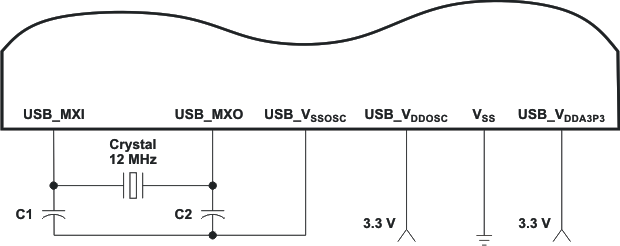 Figure 5-11 12-MHz USB Oscillator
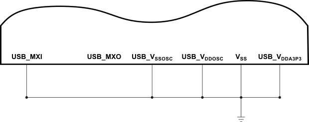 Figure 5-12 Connections when USB Oscillator is Permanently Disabled
The crystal should be in fundamental-mode operation, and parallel resonant, with a maximum effective series resistance (ESR) specified in Table 5-8. The load capacitors, C1 and C2 are the total capacitance of the circuit board and components, excluding the IC and crystal. The load capacitor value is usually approximately twice the value of the crystal's load capacitance, CL, which is specified in the crystal manufacturer's datasheet and should be chosen such that the equation below is satisfied. All discrete components used to implement the oscillator circuit should be placed as close as possible to the associated oscillator pins (USB_MXI and USB_MXO) and to the USB_VSSOSC pin.
Table 5-8 Input Requirements for Crystal on the 12-MHz USB Oscillator
| PARAMETER | MIN | NOM | MAX | UNIT | |
|---|---|---|---|---|---|
| Start-up time (from power up until oscillating at stable frequency of 12 MHz)(2) | 0.100 | 10 | ms | ||
| Oscillation frequency | 12 | MHz | |||
| ESR | 100 | kΩ | |||
| Frequency stability (1) | ±100 | ppm | |||
| Maximum shunt capacitance | 5 | pF | |||
| Maximum crystal drive | 330 | µW | |||
5.7.4.3.3.2 Real-Time Clock (RTC) On-Chip Oscillator With External Crystal
The on-chip RTC oscillator requires an external 32.768-kHz crystal connected across the RTC_XI and RTC_XO pins, along with two load capacitors, as shown in Figure 5-13. The external crystal load capacitors must be connected only to the RTC oscillator ground pin (VSSRTC). Do not connect to board ground (VSS). Position the VSS lead on the board between RTC_XI and RTC_XO as a shield to reduce direct capacitance between RTC_XI and RTC_XO leads on the board. The CVDDRTC pin can be connected to the same power supply as CVDD, or may be connected to a different supply that meets the recommended operating conditions (see Section 5.2, Recommended Operating Conditions), if desired.
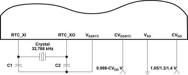 Figure 5-13 32.768-kHz RTC Oscillator
The RTC oscillator can be optionally disabled by connecting RTC_XI to CVDDRTC and RTC_XO to ground (VSS). However, when the RTC oscillator is disabled the RTC registers starting at I/O address 1900h will not be accessible. This includes the RTC Power Management Register which provides control to the on-chip LDOs and WAKEUP and RTC_CLKOUT pins. Note: The RTC must still be powered even if the RTC oscillator is disabled.
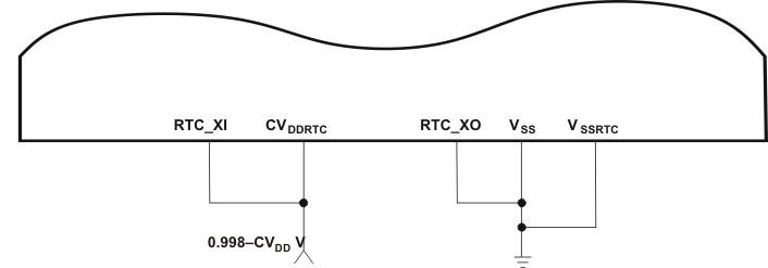 Figure 5-14 Connections when RTC Oscillator is Permanently Disabled
The crystal should be in fundamental-mode function, and parallel resonant, with a maximum effective series resistance (ESR) specified in Table 5-9. The load capacitors, C1 and C2, are the total capacitance of the circuit board and components, excluding the IC and crystal. The load capacitors values are usually approximately twice the value of the crystal's load capacitance, CL, which is specified in the crystal manufacturer's datasheet and should be chosen such that the equation is satisfied. All discrete components used to implement the oscillator circuit should be placed as close as possible to the associated oscillator pins (RTC_XI and RTC_XO) and to the VSSRTC pin.
Table 5-9 Input Requirements for Crystal on the 32.768-kHz RTC Oscillator
| PARAMETER | MIN | NOM | MAX | UNIT | |
|---|---|---|---|---|---|
| Start-up time (from power up until oscillating at stable frequency of 32.768-kHz)(1) | 0.2 | 2 | sec | ||
| Oscillation frequency | 32.768 | kHz | |||
| ESR | 100 | kΩ | |||
| Maximum shunt capacitance | 1.6 | pF | |||
| Maximum crystal drive | 1.0 | µW | |||
5.7.4.3.3.3 CLKIN Pin With LVCMOS-Compatible Clock Input (Optional)
Note: If CLKIN is not used, the pin must be tied low.
A LVCMOS-compatible clock can be fed into the CLKIN pin for use by the DSP system clock generator. The external connections are shown in Figure 5-15 and Figure 5-16. The bootloader assumes that the CLKIN pin is connected to the LVCMOS-compatible clock source with a frequency of 11.2896, 12.0, 12.288, 16.8, or 19.2 MHz based on the value of BootMode[5:4] bits at reset. (See Section 6.4, Boot Mode, for details.) Note: The CLKIN pin operates at the same voltage as the DVDDIO supply (1.8, 2.75, or 3.3 V).
In this configuration the RTC oscillator can be optionally disabled by connecting RTC_XI to CVDDRTC and RTC_XO to ground (VSS). However, when the RTC oscillator is disabled the RTC registers starting at I/O address 1900h will not be accessible. This includes the RTC Power Management Register which provides control to the on-chip LDOs and WAKEUP and RTC_CLKOUT pins. Note: The RTC must still be powered by an external power source even if the RTC oscillator is disabled. None of the on-chip LDOs can power CVDDRTC.
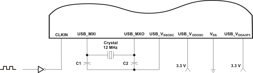 Figure 5-15 LVCMOS-Compatible Clock Input With USB Oscillator Enabled
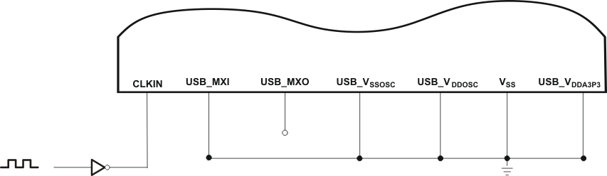 Figure 5-16 LVCMOS-Compatible Clock Input With USB Oscillator Disabled
5.7.4.4 Input and Output Clocks Electrical Data and Timing
Table 5-10 Timing Requirements for CLKIN(1)(2) (see Figure 5-17)
| NO. | CVDD = 1.05/1.3/1.4 V | UNIT | ||||
|---|---|---|---|---|---|---|
| MIN | NOM | MAX | ||||
| 1 | tc(CLKIN) | Cycle time, external clock driven on CLKIN | 11.2896 12.0, 12.288, 16.8, or 19.2 |
MHz | ||
| 2 | tw(CLKINH) | Pulse duration, CLKIN high | 0.466 * tc(CLKIN) | ns | ||
| 3 | tw(CLKINL) | Pulse duration, CLKIN low | 0.466 * tc(CLKIN) | ns | ||
| 4 | tt(CLKIN) | Transition time, CLKIN | 4 | ns | ||
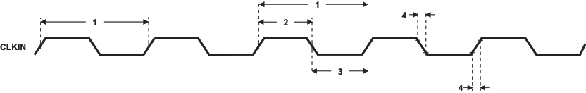 Figure 5-17 CLKIN Timing
Table 5-11 Switching Characteristics Over Recommended Operating Conditions for CLKOUT
[I/O = 3.3/2.75 V](1)(2)
(see Figure 5-18)
| NO. | PARAMETER | CVDD = 1.05/1.3/1.4 V VDDA_PLL = 1.3 V |
UNIT | |||
|---|---|---|---|---|---|---|
| MIN | MAX | |||||
| 1 | tc(CLKOUT) | Cycle time, CLKOUT | 10 | ns | ||
| 2 | tw(CLKOUTH) | Pulse duration, CLKOUT high | 0.466 * tc(CLKOUT) | ns | ||
| 3 | tw(CLKOUTL) | Pulse duration, CLKOUT low | 0.466 * tc(CLKOUT) | ns | ||
| 4 | tt(CLKOUTR) | Transition time (rise), CLKOUT | 5 | ns | ||
| 5 | tt(CLKOUTF) | Transition time (fall), CLKOUT | 5 | ns | ||
Table 5-12 Switching Characteristics Over Recommended Operating Conditions for CLKOUT
[I/O = 1.8 V](1)(2)
(see Figure 5-18)
| NO. | PARAMETER | CVDD = 1.05/1.3/1.4 V VDDA_PLL = 1.3 V |
UNIT | |||
|---|---|---|---|---|---|---|
| MIN | MAX | |||||
| 1 | tc(CLKOUT) | Cycle time, CLKOUT | 20 | ns | ||
| 2 | tw(CLKOUTH) | Pulse duration, CLKOUT high | 0.466 * tc(CLKOUT) | ns | ||
| 3 | tw(CLKOUTL) | Pulse duration, CLKOUT low | 0.466 * tc(CLKOUT) | ns | ||
| 4 | tt(CLKOUTR) | Transition time (rise), CLKOUT | 5 | ns | ||
| 5 | tt(CLKOUTF) | Transition time (fall), CLKOUT | 5 | ns | ||
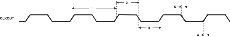 Figure 5-18 CLKOUT Timing
5.7.4.5 Wake-up Events, Interrupts, and XF
The device has a number of interrupts to service the needs of its peripherals. The interrupts can be selectively enabled or disabled.
5.7.4.5.1 Interrupts Electrical Data and Timing
Table 5-13 Timing Requirements for Interrupts(1) (see Figure 5-19)
| NO. | CVDD = 1.05 V CVDD = 1.3 V CVDD = 1.4 V |
UNIT | |||
|---|---|---|---|---|---|
| MIN | MAX | ||||
| 1 | tw(INTH) | Pulse duration, interrupt high CPU active | 2P | ns | |
| 2 | tw(INTL) | Pulse duration, interrupt low CPU active | 2P | ns | |
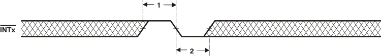 Figure 5-19 External Interrupt Timings
5.7.4.5.2 Wake-Up From IDLE Electrical Data and Timing
Table 5-14 Timing Requirements for Wake-Up From IDLE (see Figure 5-20)
| NO. | CVDD = 1.05 V CVDD = 1.3 V CVDD = 1.4 V |
UNIT | |||
|---|---|---|---|---|---|
| MIN | MAX | ||||
| 1 | tw(WKPL) | Pulse duration, WAKEUP or INTx low, SYSCLKDIS = 1 | 30.5 | μs | |
Table 5-15 Switching Characteristics Over Recommended Operating Conditions For Wake-Up From IDLE(1)(2)(3)(4) (see Figure 5-20)
| NO. | PARAMETER | CVDD = 1.05 V CVDD = 1.3 V CVDD = 1.4 V |
UNIT | ||||
|---|---|---|---|---|---|---|---|
| MIN | TYP | MAX | |||||
| 2 | td(WKEVTH-CKLGEN) | Delay time, WAKEUP pulse complete to CPU active | IDLE3 Mode(5) with SYSCLKDIS = 1, WAKEUP or INTx event, CLK_SEL = 1 | D | ns | ||
| IDLE3 Mode(5) with SYSCLKDIS = 1, WAKEUP or INTx event, CLK_SEL = 0 | C | ns | |||||
| IDLE2 Mode(5); INTx event | 3P | ns | |||||
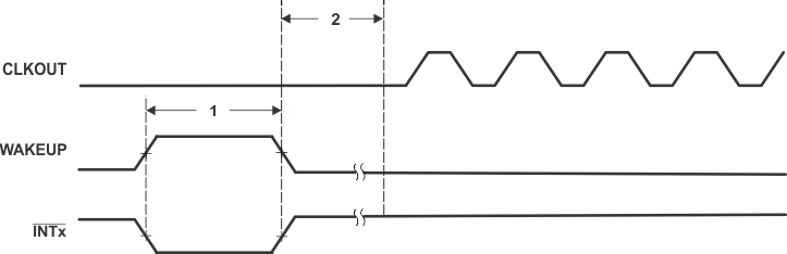
For a description of IDLE2 and IDLE3 mode, see the System chapter in the TMS320C5517 Digital Signal Processor Technical Reference Manual [literature number SPRUH16].
5.7.4.5.3 XF Electrical Data and Timing
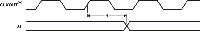
Table 5-16 Switching Characteristics Over Recommended Operating Conditions For XF(3)(2)
(see Figure 5-21)
| NO. | PARAMETER | CVDD = 1.05 V CVDD = 1.3 V CVDD = 1.4 V |
UNIT | |||
|---|---|---|---|---|---|---|
| MIN | MAX | |||||
| 1 | td(XF) | Delay time, CLKOUT high to XF high | 0 | 10.2 | ns | |
5.7.5 Direct Memory Access (DMA) Controller
The DMA controller is used to move data among internal memory, external memory, and peripherals without intervention from the CPU and in the background of CPU operation.
The DSP includes a total of four DMA controllers. Aside from the DSP resources they can access, all four DMA controllers are identical.
The DMA controller has the following features:
- Operation that is independent of the CPU.
- Four channels, which allow the DMA controller to keep track of the context of four independent block transfers.
- Event synchronization. DMA transfers in each channel can be made dependent on the occurrence of selected events.
- An interrupt for each channel. Each channel can send an interrupt to the CPU on completion of the programmed transfer.
- Ping-Pong mode allows the DMA controller to keep track of double buffering context without CPU intervention.
- A dedicated clock idle domain. The four device DMA controllers can be put into a low-power state by independently turning off their input clocks.
5.7.5.1 DMA Channel Synchronization Events
The DMA controllers allow activity in their channels to be synchronized to selected events. The DSP supports 20 separate synchronization events and each channel can be tied to separate sync events independent of the other channels. Synchronization events are selected by programming the CHnEVT field in the DMAn channel event source registers (DMAnCESR1 and DMAnCESR2).
5.7.6 External Memory Interface (EMIF)
The device supports several memories and external device interfaces, including: NOR Flash, NAND Flash, SRAM, Non-Mobile SDRAM, and Mobile SDRAM (mSDRAM).
Note: The device can support non-mobile SDRAM under certain circumstances. The device also always uses mobile SDRAM initialization, but it is able to support SDRAM memories that ignore the BA0 and BA1 pins for the 'load mode register' command. During the mobile SDRAM initialization, the device issues the 'load mode register' initialization command to two different addresses that differ in only the BA0 and BA1 address bits. These registers are the Extended Mode register and the Mode register. The Extended mode register exists only in mSDRAM and not in non-mSDRAM. If a non-mobile SDRAM memory ignores bits BA0 and BA1, the second loaded register value overwrites the first, leaving the desired value in the Mode register and the non-mobile SDRAM will work with the device.
The EMIF provides an 8-bit or 16-bit data bus, an address bus width up to 21 bits, and 6 chip selects, along with memory control signals.
The EM_A[20:15] address signals are multiplexed with the GPIO peripheral and controlled by the External Bus Selection Register (EBSR). For more detail on the pin muxing, see Section 5.7.3.5.1, External Bus Selection Register (EBSR).
5.7.6.1 EMIF Asynchronous Memory Support
The EMIF supports asynchronous:
- SRAM memories
- NAND Flash memories
- NOR Flash memories
The EMIF data bus can be configured for both 8- or 16-bit width. The device supports up to 21 address lines and four external wait and interrupt inputs. Up to four asynchronous chip selects are supported by EMIF (EM_CS[5:2]).
Each chip select has the following individually programmable attributes:
- Data bus width
- Read cycle timings: setup, hold, strobe
- Write cycle timings: setup, hold, strobe
- Bus turn around time
- Select Strobe Option
- NAND flash controller supports 1-bit and 4-bit ECC calculation on blocks of 512 bytes
Each chip select shares the following programmable attribute: Extended Wait Option with Programmable Timeout.
5.7.6.2 EMIF Non-Mobile and Mobile Synchronous DRAM Memory Supported
The EMIF supports 16-bit non-mobile and mobile single data rate (SDR) SDRAM in addition to the asynchronous memories listed in Section 5.7.6.1, EMIF Asynchronous Memory Support. The supported SDRAM and mobile SDRAM configurations are:
- One, two, and four bank SDRAM and mSDRAM devices
- Supports devices with eight, nine, ten, and eleven column addresses
- CAS latency of two or three clock cycles
- 16-bit data-bus width
- 3.3-, 2.75-, and 1.8 -V LVCMOS interface that is separate from the rest of the chip I/Os.
- One (EM_CS0) or two (EM_CS[1:0]) chip selects
Additionally, the SDRAM and mSDRAM interface of EMIF supports placing the SDRAM and mSDRAM in "Self-Refresh" and "Powerdown Modes". Self-Refresh mode allows the SDRAM and mSDRAM to be put into a low-power state while still retaining memory contents; since the SDRAM and mSDRAM will continue to refresh itself even without clocks from the DSP. Powerdown mode achieves even lower power, except the DSP must periodically wake the SDRAM and mSDRAM up and issue refreshes if data retention is required. To achieve the lowest power consumption, the SDRAM and mSDRAM interface has configurable slew rate on the EMIF pins.
The device has limitations to the clock frequency on the EM_SDCLK pin based on the CVDD and DVDDEMIF:
- The clock frequency on the EM_SDCLK pin can be configured either as SYSCLK (DSP operating frequency) or SYSCLK/2 via bit 0 of the ECDR Register (1C26h).
- When CVDD = 1.3 V or 1.4 V, and DVDDEMIF = 3.3 V or 2.75 V, the max clock frequency on the EM_SDCLK pin is limited to 100 MHz (EM_SDCLK = 100 MHz). Therefore, if SYSCLK ≤ 100 MHz, the EM_SDCLK can be configured either as SYSCLK or SYSCLK/2. If SYSCLK > 100 MHz, the EM_SDCLK must be configured as SYSCLK/2 and ≤ 100 MHz.
- When CVDD =1.05 V, and DVDDEMIF = 3.3 V or 2.75 V, the max clock frequency on the EM_SDCLK pin is limited to 75 MHz (EM_SDCLK = 75 MHz). Therefore, if SYSCLK ≤ 75 MHz, the EM_SDCLK can be configured as either SYSCLK or SYSCLK/2. If SYSCLK > 75 MHz, the EM_SDCLK must be configured as SYSCLK/2 and ≤ 75 MHz.
- When DVDDEMIF = 1.8 V, regardless of the CVDD voltage, the clock frequency on the EM_SDCLK pin must be configured as SYSCLK/2 and ≤ 50 MHz.
5.7.6.3 EMIF Electrical Data and Timing CVDD = 1.05 V, DVDDEMIF = 3.3/2.75/1.8 V
Table 5-17 Timing Requirements for EMIF SDRAM and mSDRAM Interface(1) (see Figure 5-22 and Figure 5-23)
| NO. | CVDD = 1.05 V DVDDEMIF = 3.3/2.75 V |
CVDD = 1.05 V DVDDEMIF = 1.8 V |
UNIT | |||||||
|---|---|---|---|---|---|---|---|---|---|---|
| MIN | MAX | MIN | MAX | |||||||
| 19 | tsu(DV-CLKH) | Input setup time, read data valid on EM_D[15:0] before EM_SDCLK rising | 4.07 | 5.86 | ns | |||||
| 20 | th(CLKH-DIV) | Input hold time, read data valid on EM_D[15:0] after EM_SDCLK rising | 2.1 | 2.6 | ns | |||||
Table 5-18 Switching Characteristics Over Recommended Operating Conditions for EMIF SDRAM and mSDRAM Interface(1)(2) (see Figure 5-22 and Figure 5-23)
| NO. | PARAMETER | CVDD = 1.05 V DVDDEMIF = 3.3/2.75 V |
CVDD = 1.05 V DVDDEMIF = 1.8 V |
UNIT | ||||||||
|---|---|---|---|---|---|---|---|---|---|---|---|---|
| MIN | TYP | MAX | MIN | TYP | MAX | |||||||
| 1 | tc(CLK) | Cycle time, EMIF clock EM_SDCLK | 13.33(3) | 20(4) | ns | |||||||
| 2 | tw(CLK) | Pulse duration, EMIF clock EM_SDCLK high or low | 6.67 | 10 | ns | |||||||
| 3 | td(CLKH-CSV) | Delay time, EM_SDCLK rising to EMA_CS[1:0] valid | 1.1 | 10.67 | 1.1 | 13.46 | ns | |||||
| 5 | td(CLKH-DQMV) | Delay time, EM_SDCLK rising to EM_DQM[1:0] valid | 1.1 | 10.67 | 1.1 | 13.46 | ns | |||||
| 7 | td(CLKH-AV) | Delay time, EM_SDCLK rising to EM_A[20:0] and EM_BA[1:0] valid | 1.1 | 10.67 | 1.1 | 13.46 | ns | |||||
| 9 | td(CLKH-DV) | Delay time, EM_SDCLK rising to EM_D[15:0] valid | 1.1 | 10.67 | 1.1 | 13.46 | ns | |||||
| 11 | td(CLKH-RASV) | Delay time, EM_SDCLK rising to EM_SDRAS valid | 1.1 | 10.67 | 1.1 | 13.46 | ns | |||||
| 13 | td(CLKH-CASV) | Delay time, EM_SDCLK rising to EM_SDCAS valid | 1.1 | 10.67 | 1.1 | 13.46 | ns | |||||
| 15 | td(CLKH-WEV) | Delay time, EM_SDCLK rising to EM_WE valid | 1.1 | 10.67 | 1.1 | 13.46 | ns | |||||
| 21 | td(CLKH-CKEV) | Delay time, EM_SDCLK rising to EM_SDCKE valid | 1.1 | 10.67 | 1.1 | 13.46 | ns | |||||
Table 5-19 Timing Requirements for EMIF Asynchronous Memory, DVDDEMIF = 1.8 V(1)(2) (see Figure 5-24, Figure 5-26, and Figure 5-27)
| NO. | CVDD = 1.05 V DVDDEMIF = 1.8 V |
UNIT | ||||
|---|---|---|---|---|---|---|
| MIN | NOM | MAX | ||||
| READS and WRITES | ||||||
| 2 | tw(EM_WAIT) | Pulse duration, EM_WAITx assertion and deassertion | 2E | ns | ||
| READS | ||||||
| 12 | tsu(EMDV-EMOEH) | Setup time, EM_D[15:0] valid before EM_OE high | 18 | ns | ||
| 13 | th(EMOEH-EMDIV) | Hold time, EM_D[15:0] valid after EM_OE high | 0 | ns | ||
| 14 | tsu(EMOEL-EMWAIT) | Setup time, EM_WAITx asserted before end of Strobe Phase(3) | 4E + 18 | ns | ||
| WRITES | ||||||
| 28 | tsu(EMWEL-EMWAIT) | Setup time, EM_WAITx asserted before end of Strobe Phase(3) | 4E + 18 | ns | ||
Table 5-20 Timing Requirements for EMIF Asynchronous Memory, DVDDEMIF = 3.3/2.75 V(1)(2) (see Figure 5-24, Figure 5-26, and Figure 5-27)
| NO. | CVDD = 1.05 V DVDDEMIF = 3.3/2.75 V |
UNIT | ||||
|---|---|---|---|---|---|---|
| MIN | NOM | MAX | ||||
| READS and WRITES | ||||||
| 2 | tw(EM_WAIT) | Pulse duration, EM_WAITx assertion and deassertion | 2E | ns | ||
| READS | ||||||
| 12 | tsu(EMDV-EMOEH) | Setup time, EM_D[15:0] valid before EM_OE high | 17 | ns | ||
| 13 | th(EMOEH-EMDIV) | Hold time, EM_D[15:0] valid after EM_OE high | 0 | ns | ||
| 14 | tsu(EMOEL-EMWAIT) | Setup time, EM_WAITx asserted before end of Strobe Phase(3) | 4E + 17 | ns | ||
| WRITES | ||||||
| 28 | tsu(EMWEL-EMWAIT) | Setup time, EM_WAITx asserted before end of Strobe Phase(3) | 4E + 17 | ns | ||
Table 5-21 Switching Characteristics Over Recommended Operating Conditions for EMIF Asynchronous Memory, DVDDEMIF = 1.8 V(1)(2)(3) (see Figure 5-25 and Figure 5-27)(4)
| NO. | PARAMETER | CVDD = 1.05 V DVDDEMIF = 1.8 V |
UNIT | |||
|---|---|---|---|---|---|---|
| MIN | TYP | MAX | ||||
| READS and WRITES | ||||||
| 1 | td(TURNAROUND) | Turn around time | (TA)*E - 18 | (TA)*E | (TA)*E + 18 | ns |
| READS | ||||||
| 3 | tc(EMRCYCLE) | EMIF read cycle time (EW = 0) | (RS+RST+RH)*E - 18 | (RS+RST+RH)*E | (RS+RST+RH)*E + 18 | ns |
| EMIF read cycle time (EW = 1) | (RS+RST+RH+(EWC*16))*E - 18 | (RS+RST+RH+(EWC*16))*E | (RS+RST+RH+(EWC*16))*E + 18 | ns | ||
| 4 | tsu(EMCEL-EMOEL) | Output setup time, EM_CS[5:2] low to EM_OE low (SS = 0) | (RS)*E - 11 | (RS)*E | (RS)*E + 11 | ns |
| Output setup time, EM_CS[5:2] low to EM_OE low (SS = 1) | -11 | 0 | +11 | ns | ||
| 5 | th(EMOEH-EMCEH) | Output hold time, EM_OE high to EM_CS[5:2] high (SS = 0) | (RH)*E - 11 | (RH)*E | (RH)*E + 11 | ns |
| Output hold time, EM_OE high to EM_CS[5:2] high (SS = 1) | -11 | 0 | +11 | ns | ||
| 6 | tsu(EMBAV-EMOEL) | Output setup time, EM_BA[1:0] valid to EM_OE low | (RS)*E - 11 | (RS)*E | (RS)*E + 11 | ns |
| 7 | th(EMOEH-EMBAIV) | Output hold time, EM_OE high to EM_BA[1:0] invalid | (RH)*E - 18 | (RH)*E | (RH)*E + 18 | ns |
| 8 | tsu(EMBAV-EMOEL) | Output setup time, EM_A[20:0] valid to EM_OE low | (RS)*E - 11 | (RS)*E | (RS)*E + 11 | ns |
| 9 | th(EMOEH-EMAIV) | Output hold time, EM_OE high to EM_A[20:0] invalid | (RH)*E - 18 | (RH)*E | (RH)*E + 18 | ns |
| 10 | tw(EMOEL) | EM_OE active low pulse (EW = 0) | (RST)*E - 18 | (RST)*E | (RST)*E + 18 | ns |
| EM_OE active low pulse (EW = 1) | (RST+(EWC*16))*E - 18 | (RST+(EWC*16))*E | (RST+(EWC*16))*E + 11 | ns | ||
| 11 | td(EMWAITH-EMOEH) | Delay time from EM_WAITx deasserted to EM_OE high | 4E - 18 | 4E | 4E + 18 | ns |
| WRITES | ||||||
| 15 | tc(EMWCYCLE) | EMIF write cycle time (EW = 0) | (WS+WST+WH)*E - 18 | (WS+WST+WH)*E | (WS+WST+WH)*E + 18 | ns |
| EMIF write cycle time (EW = 1) | (WS+WST+WH+(EWC*16))*E - 18 | (WS+WST+WH+(EWC*16))*E | (WS+WST+WH+(EWC*16))*E + 18 | ns | ||
| 16 | tsu(EMCSL-EMWEL) | Output setup time, EM_CS[5:2] low to EM_WE low (SS = 0) | (WS)*E - 18 | (WS)*E | (WS)*E + 18 | ns |
| Output setup time, EM_CS[5:2] low to EM_WE low (SS = 1) | -18 | 0 | +18 | ns | ||
| 17 | th(EMWEH-EMCSH) | Output hold time, EM_WE high to EM_CS[5:2] high (SS = 0) | (WH)*E - 11 | (WH)*E | (WH)*E + 11 | ns |
| Output hold time, EM_WE high to EM_CS[5:2] high (SS = 1) | -11 | 0 | +11 | ns | ||
| 18 | tsu(EMBAV-EMWEL) | Output setup time, EM_BA[1:0] valid to EM_WE low | (WS)*E - 11 | (WS)*E | (WS)*E + 11 | ns |
| 19 | th(EMWEH-EMBAIV) | Output hold time, EM_WE high to EM_BA[1:0] invalid | (WH)*E - 11 | (WH)*E | (WH)*E + 11 | ns |
| 20 | tsu(EMAV-EMWEL) | Output setup time, EM_A[20:0] valid to EM_WE low | (WS)*E - 11 | (WS)*E | (WS)*E + 11 | ns |
| 21 | th(EMWEH-EMAIV) | Output hold time, EM_WE high to EM_A[20:0] invalid | (WH)*E - 11 | (WH)*E | (WH)*E + 11 | ns |
| 22 | tw(EMWEL) | EM_WE active low pulse (EW = 0) | (WST)*E - 18 | (WST)*E | (WST)*E + 18 | ns |
| EM_WE active low pulse (EW = 1) | (WST+(EWC*16))*E - 18 | (WST+(EWC*16))*E | (WST+(EWC*16))*E + 18 | ns | ||
| 23 | td(EMWAITH-EMWEH) | Delay time from EM_WAITx deasserted to EM_WE high | 3E - 18 | 4E | 4E + 18 | ns |
| 24 | tsu(EMDV-EMWEL) | Output setup time, EM_D[15:0] valid to EM_WE low | (WS)*E - 18 | (WS)*E | (WS)*E + 18 | ns |
| 25 | th(EMWEH-EMDIV) | Output hold time, EM_WE high to EM_D[15:0] invalid | (WH)*E - 11 | (WH)*E | (WH)*E + 11 | ns |
Table 5-22 Switching Characteristics Over Recommended Operating Conditions for EMIF Asynchronous Memory, DVDDEMIF = 3.3/2.75 V(1)(2)(3) (see Figure 5-25 and Figure 5-27)(4)
| NO. | PARAMETER | CVDD = 1.05 V DVDDEMIF = 3.3/2.75 V |
UNIT | |||
|---|---|---|---|---|---|---|
| MIN | TYP | MAX | ||||
| READS and WRITES | ||||||
| 1 | td(TURNAROUND) | Turn around time | (TA)*E - 17 | (TA)*E | (TA)*E + 17 | ns |
| READS | ||||||
| 3 | tc(EMRCYCLE) | EMIF read cycle time (EW = 0) | (RS+RST+RH)*E - 17 | (RS+RST+RH)*E | (RS+RST+RH)*E + 17 | ns |
| EMIF read cycle time (EW = 1) | (RS+RST+RH+(EWC*16))*E - 17 | (RS+RST+RH+(EWC*16))*E | (RS+RST+RH+(EWC*16))*E + 17 | ns | ||
| 4 | tsu(EMCEL-EMOEL) | Output setup time, EM_CS[5:2] low to EM_OE low (SS = 0) | (RS)*E - 9 | (RS)*E | (RS)*E + 9 | ns |
| Output setup time, EM_CS[5:2] low to EM_OE low (SS = 1) | -9 | 0 | +9 | ns | ||
| 5 | th(EMOEH-EMCEH) | Output hold time, EM_OE high to EM_CS[5:2] high (SS = 0) | (RH)*E - 9 | (RH)*E | (RH)*E + 9 | ns |
| Output hold time, EM_OE high to EM_CS[5:2] high (SS = 1) | -9 | 0 | +9 | ns | ||
| 6 | tsu(EMBAV-EMOEL) | Output setup time, EM_BA[1:0] valid to EM_OE low | (RS)*E - 9 | (RS)*E | (RS)*E + 9 | ns |
| 7 | th(EMOEH-EMBAIV) | Output hold time, EM_OE high to EM_BA[1:0] invalid | (RH)*E - 17 | (RH)*E | (RH)*E + 17 | ns |
| 8 | tsu(EMBAV-EMOEL) | Output setup time, EM_A[20:0] valid to EM_OE low | (RS)*E - 9 | (RS)*E | (RS)*E + 9 | ns |
| 9 | th(EMOEH-EMAIV) | Output hold time, EM_OE high to EM_A[20:0] invalid | (RH)*E - 17 | (RH)*E | (RH)*E + 17 | ns |
| 10 | tw(EMOEL) | EM_OE active low pulse (EW = 0) | (RST)*E - 17 | (RST)*E | (RST)*E + 17 | ns |
| EM_OE active low pulse (EW = 1) | (RST+(EWC*16))*E - 17 | (RST+(EWC*16))*E | (RST+(EWC*16))*E + 9 | ns | ||
| 11 | td(EMWAITH-EMOEH) | Delay time from EM_WAITx deasserted to EM_OE high | 4E - 17 | 4E | 4E + 17 | ns |
| WRITES | ||||||
| 15 | tc(EMWCYCLE) | EMIF write cycle time (EW = 0) | (WS+WST+WH)*E - 17 | (WS+WST+WH)*E | (WS+WST+WH)*E + 17 | ns |
| EMIF write cycle time (EW = 1) | (WS+WST+WH+(EWC*16))*E - 17 | (WS+WST+WH+(EWC*16))*E | (WS+WST+WH+(EWC*16))*E + 17 | ns | ||
| 16 | tsu(EMCSL-EMWEL) | Output setup time, EM_CS[5:2] low to EM_WE low (SS = 0) | (WS)*E - 17 | (WS)*E | (WS)*E + 17 | ns |
| Output setup time, EM_CS[5:2] low to EM_WE low (SS = 1) | -17 | 0 | +17 | ns | ||
| 17 | th(EMWEH-EMCSH) | Output hold time, EM_WE high to EM_CS[5:2] high (SS = 0) | (WH)*E - 9 | (WH)*E | (WH)*E + 9 | ns |
| Output hold time, EM_WE high to EM_CS[5:2] high (SS = 1) | -9 | 0 | +9 | ns | ||
| 18 | tsu(EMBAV-EMWEL) | Output setup time, EM_BA[1:0] valid to EM_WE low | (WS)*E - 9 | (WS)*E | (WS)*E + 9 | ns |
| 19 | th(EMWEH-EMBAIV) | Output hold time, EM_WE high to EM_BA[1:0] invalid | (WH)*E - 9 | (WH)*E | (WH)*E + 9 | ns |
| 20 | tsu(EMAV-EMWEL) | Output setup time, EM_A[20:0] valid to EM_WE low | (WS)*E - 9 | (WS)*E | (WS)*E + 9 | ns |
| 21 | th(EMWEH-EMAIV) | Output hold time, EM_WE high to EM_A[20:0] invalid | (WH)*E - 9 | (WH)*E | (WH)*E + 9 | ns |
| 22 | tw(EMWEL) | EM_WE active low pulse (EW = 0) | (WST)*E - 17 | (WST)*E | (WST)*E + 17 | ns |
| EM_WE active low pulse (EW = 1) | (WST+(EWC*16))*E - 17 | (WST+(EWC*16))*E | (WST+(EWC*16))*E + 17 | ns | ||
| 23 | td(EMWAITH-EMWEH) | Delay time from EM_WAITx deasserted to EM_WE high | 3E - 17 | 4E | 4E + 17 | ns |
| 24 | tsu(EMDV-EMWEL) | Output setup time, EM_D[15:0] valid to EM_WE low | (WS)*E - 17 | (WS)*E | (WS)*E + 17 | ns |
| 25 | th(EMWEH-EMDIV) | Output hold time, EM_WE high to EM_D[15:0] invalid | (WH)*E - 9 | (WH)*E | (WH)*E + 9 | ns |
5.7.6.4 EMIF Electrical Data and Timing CVDD = 1.3/1.4 V, DVDDEMIF = 3.3/2.75/1.8 V
Table 5-23 Timing Requirements for EMIF SDRAM and mSDRAM Interface(1) (see Figure 5-22 and Figure 5-23)
| NO. | CVDD = 1.3/1.4 V DVDDEMIF = 3.3/2.75 V |
CVDD = 1.3/1.4 V DVDDEMIF = 1.8 V |
UNIT | |||||||
|---|---|---|---|---|---|---|---|---|---|---|
| MIN | MAX | MIN | MAX | |||||||
| 19 | tsu(DV-CLKH) | Input setup time, read data valid on EM_D[15:0] before EM_SDCLK rising | 4.07 | 3.28 | ns | |||||
| 20 | th(CLKH-DIV) | Input hold time, read data valid on EM_D[15:0] after EM_SDCLK rising | 2.1 | 3.1 | ns | |||||
Table 5-24 Switching Characteristics Over Recommended Operating Conditions for EMIF SDRAM and mSDRAM Interface(1)(2) (see Figure 5-22 and Figure 5-23)
| NO. | PARAMETER | CVDD = 1.3/1.4 V DVDDEMIF = 3.3/2.75 V |
CVDD = 1.3/1.4 V DVDDEMIF = 1.8 V |
UNIT | ||||||||
|---|---|---|---|---|---|---|---|---|---|---|---|---|
| MIN | TYP | MAX | MIN | TYP | MAX | |||||||
| 1 | tc(CLK) | Cycle time, EMIF clock EM_SDCLK | 10(3) | 20(4) | ns | |||||||
| 2 | tw(CLK) | Pulse duration, EMIF clock EM_SDCLK high or low | 5 | 10 | ns | |||||||
| 3 | td(CLKH-CSV) | Delay time, EM_SDCLK rising to EMA_CS[1:0] valid | 0.9 | 7.88 | 1.1 | 10.67 | ns | |||||
| 5 | td(CLKH-DQMV) | Delay time, EM_SDCLK rising to EM_DQM[1:0] valid | 0.9 | 7.88 | 1.1 | 10.67 | ns | |||||
| 7 | td(CLKH-AV) | Delay time, EM_SDCLK rising to EM_A[20:0] and EM_BA[1:0] valid | 0.9 | 7.88 | 1.1 | 10.67 | ns | |||||
| 9 | td(CLKH-DV) | Delay time, EM_SDCLK rising to EM_D[15:0] valid | 0.9 | 7.88 | 1.1 | 10.67 | ns | |||||
| 11 | td(CLKH-RASV) | Delay time, EM_SDCLK rising to EM_SDRAS valid | 0.9 | 7.88 | 1.1 | 10.67 | ns | |||||
| 13 | td(CLKH-CASV) | Delay time, EM_SDCLK rising to EM_SDCAS valid | 0.9 | 7.88 | 1.1 | 10.67 | ns | |||||
| 15 | td(CLKH-WEV) | Delay time, EM_SDCLK rising to EM_WE valid | 0.9 | 7.88 | 1.1 | 10.67 | ns | |||||
| 21 | td(CLKH-CKEV) | Delay time, EM_SDCLK rising to EM_SDCKE valid | 0.9 | 7.88 | 1.1 | 10.67 | ns | |||||
Table 5-25 Timing Requirements for EMIF Asynchronous Memory, DVDDEMIF = 1.8 V(1)(2) (see Figure 5-24, Figure 5-26, and Figure 5-27)
| NO. | CVDD = 1.3/1.4 V DVDDEMIF = 1.8 V |
UNIT | ||||
|---|---|---|---|---|---|---|
| MIN | NOM | MAX | ||||
| READS and WRITES | ||||||
| 2 | tw(EM_WAIT) | Pulse duration, EM_WAITx assertion and deassertion | 2E | ns | ||
| READS | ||||||
| 12 | tsu(EMDV-EMOEH) | Setup time, EM_D[15:0] valid before EM_OE high | 11 | ns | ||
| 13 | th(EMOEH-EMDIV) | Hold time, EM_D[15:0] valid after EM_OE high | 0 | ns | ||
| 14 | tsu(EMOEL-EMWAIT) | Setup Time, EM_WAITx asserted before end of Strobe Phase(3) | 4E + 10 | ns | ||
| WRITES | ||||||
| 28 | tsu(EMWEL-EMWAIT) | Setup Time, EM_WAITx asserted before end of Strobe Phase(3) | 4E + 10 | ns | ||
Table 5-26 Timing Requirements for EMIF Asynchronous Memory, DVDDEMIF = 3.3/2.75 V(1)(2) (see Figure 5-24, Figure 5-26, and Figure 5-27)
| NO. | CVDD = 1.3/1.4 V DVDDEMIF = 3.3/2.75 V |
UNIT | ||||
|---|---|---|---|---|---|---|
| MIN | NOM | MAX | ||||
| READS and WRITES | ||||||
| 2 | tw(EM_WAIT) | Pulse duration, EM_WAITx assertion and deassertion | 2E | ns | ||
| READS | ||||||
| 12 | tsu(EMDV-EMOEH) | Setup time, EM_D[15:0] valid before EM_OE high | 11 | ns | ||
| 13 | th(EMOEH-EMDIV) | Hold time, EM_D[15:0] valid after EM_OE high | 0 | ns | ||
| 14 | tsu(EMOEL-EMWAIT) | Setup Time, EM_WAITx asserted before end of Strobe Phase(3) | 4E + 9 | ns | ||
| WRITES | ||||||
| 28 | tsu(EMWEL-EMWAIT) | Setup Time, EM_WAITx asserted before end of Strobe Phase(3) | 4E + 9 | ns | ||
Table 5-27 Switching Characteristics Over Recommended Operating Conditions for EMIF Asynchronous Memory, DVDDEMIF = 1.8 V(1)(2)(3)(4) (see Figure 5-24, Figure 5-26, and Figure 5-27)
| NO. | PARAMETER | CVDD = 1.3/1.4 V DVDDEMIF = 1.8 V |
UNIT | |||
|---|---|---|---|---|---|---|
| MIN | TYP | MAX | ||||
| READS and WRITES | ||||||
| 1 | td(TURNAROUND) | Turn around time | (TA)*E - 10 | (TA)*E | (TA)*E + 10 | ns |
| READS | ||||||
| 3 | tc(EMRCYCLE) | EMIF read cycle time (EW = 0) | (RS+RST+RH)*E - 10 | (RS+RST+RH)*E | (RS+RST+RH)*E + 10 | ns |
| EMIF read cycle time (EW = 1) | (RS+RST+RH+(EWC*16))*E - 10 | (RS+RST+RH+(EWC*16))*E | (RS+RST+RH+(EWC*16))*E + 10 | ns | ||
| 4 | tsu(EMCSL-EMOEL) | Output setup time, EM_CS[5:2] low to EM_OE low (SS = 0) | (RS)*E - 4 | (RS)*E | (RS)*E + 4 | ns |
| Output setup time, EM_CS[5:2] low to EM_OE low (SS = 1) | -4 | 0 | +4 | ns | ||
| 5 | th(EMOEH-EMCSH) | Output hold time, EM_OE high to EM_CS[5:2] high (SS = 0) | (RH)*E - 4 | (RH)*E | (RH)*E + 4 | ns |
| Output hold time, EM_OE high to EM_CE[5:2] high (SS = 1) | -4 | 0 | +4 | ns | ||
| 6 | tsu(EMBAV-EMOEL) | Output setup time, EM_BA[1:0] valid to EM_OE low | (RS)*E - 4 | (RS)*E | (RS)*E + 4 | ns |
| 7 | th(EMOEH-EMBAIV) | Output hold time, EM_OE high to EM_BA[1:0] invalid | (RH)*E - 10 | (RH)*E | (RH)*E + 10 | ns |
| 8 | tsu(EMAV-EMOEL) | Output setup time, EM_A[20:0] valid to EM_OE low | (RS)*E - 4 | (RS)*E | (RS)*E + 4 | ns |
| 9 | th(EMOEH-EMAIV) | Output hold time, EM_OE high to EM_A[20:0] invalid | (RH)*E - 10 | (RH)*E | (RH)*E + 10 | ns |
| 10 | tw(EMOEL) | EM_OE active low pulse (EW = 0) | (RST)*E - 10 | (RST)*E | (RST)*E + 10 | ns |
| EM_OE active low pulse (EW = 1) | (RST+(EWC*16))*E - 10 | (RST+(EWC*16))*E | (RST+(EWC*16))*E + 10 | ns | ||
| 11 | td(EMWAITH-EMOEH) | Delay time from EM_WAITx deasserted to EM_OE high | 4E - 10 | 4E | 4E + 10 | ns |
| WRITES | ||||||
| 15 | tc(EMWCYCLE) | EMIF write cycle time (EW = 0) | (WS+WST+WH)*E - 10 | (WS+WST+WH)*E | (WS+WST+WH)*E + 10 | ns |
| EMIF write cycle time (EW = 1) | (WS+WST+WH+(EWC*16))*E - 10 | (WS+WST+WH+(EWC*16))*E | (WS+WST+WH+(EWC*16))*E + 10 | ns | ||
| 16 | tsu(EMCSL-EMWEL) | Output setup time, EM_CS[5:2] low to EM_WE low (SS = 0) | (WS)*E - 10 | (WS)*E | (WS)*E +10 | ns |
| Output setup time, EM_CS[5:2] low to EM_WE low (SS = 1) | -10 | 0 | +10 | ns | ||
| 17 | th(EMWEH-EMCSH) | Output hold time, EM_WE high to EM_CS[5:2] high (SS = 0) | (WH)*E - 4 | (WH)*E | (WH)*E + 4 | ns |
| Output hold time, EM_WE high to EM_CS[5:2] high (SS = 1) | -4 | 0 | +4 | ns | ||
| 18 | tsu(EMBAV-EMWEL) | Output setup time, EM_BA[1:0] valid to EM_WE low | (WS)*E - 4 | (WS)*E | (WS)*E + 4 | ns |
| 19 | th(EMWEH-EMBAIV) | Output hold time, EM_WE high to EM_BA[1:0] invalid | (WH)*E - 4 | (WH)*E | (WH)*E + 4 | ns |
| 20 | tsu(EMAV-EMWEL) | Output setup time, EM_A[20:0] valid to EM_WE low | (WS)*E - 4 | (WS)*E | (WS)*E + 4 | ns |
| 21 | th(EMWEH-EMAIV) | Output hold time, EM_WE high to EM_A[20:0] invalid | (WH)*E - 4 | (WH)*E | (WH)*E + 4 | ns |
| 22 | tw(EMWEL) | EM_WE active low pulse (EW = 0) | (WST)*E - 10 | (WST)*E | (WST)*E + 10 | ns |
| EM_WE active low pulse (EW = 1) | (WST+(EWC*16))*E - 10 | (WST+(EWC*16))*E | (WST+(EWC*16))*E + 10 | ns | ||
| 23 | td(EMWAITH-EMWEH) | Delay time from EM_WAITx deasserted to EM_WE high | 3E - 10 | 4E | 4E + 10 | ns |
| 24 | tsu(EMDV-EMWEL) | Output setup time, EM_D[15:0] valid to EM_WE low | (WS)*E - 10 | (WS)*E | (WS)*E + 10 | ns |
| 25 | th(EMWEH-EMDIV) | Output hold time, EM_WE high to EM_D[15:0] invalid | (WH)*E - 4 | (WH)*E | (WH)*E + 4 | ns |
Table 5-28 Switching Characteristics Over Recommended Operating Conditions for EMIF Asynchronous Memory, DVDDEMIF = 3.3/2.75 V(1)(2)(3)(4) (see Figure 5-24, Figure 5-26, and Figure 5-27)
| NO. | PARAMETER | CVDD = 1.3/1.4 V DVDDEMIF = 3.3/2.75 V |
UNIT | |||
|---|---|---|---|---|---|---|
| MIN | TYP | MAX | ||||
| READS and WRITES | ||||||
| 1 | td(TURNAROUND) | Turn around time | (TA)*E - 9 | (TA)*E | (TA)*E + 9 | ns |
| READS | ||||||
| 3 | tc(EMRCYCLE) | EMIF read cycle time (EW = 0) | (RS+RST+RH)*E - 9 | (RS+RST+RH)*E | (RS+RST+RH)*E + 9 | ns |
| EMIF read cycle time (EW = 1) | (RS+RST+RH+(EWC*16))*E - 9 | (RS+RST+RH+(EWC*16))*E | (RS+RST+RH+(EWC*16))*E + 9 | ns | ||
| 4 | tsu(EMCSL-EMOEL) | Output setup time, EM_CS[5:2] low to EM_OE low (SS = 0) | (RS)*E - 4 | (RS)*E | (RS)*E + 4 | ns |
| Output setup time, EM_CS[5:2] low to EM_OE low (SS = 1) | -4 | 0 | +4 | ns | ||
| 5 | th(EMOEH-EMCSH) | Output hold time, EM_OE high to EM_CS[5:2] high (SS = 0) | (RH)*E - 4 | (RH)*E | (RH)*E + 4 | ns |
| Output hold time, EM_OE high to EM_CE[5:2] high (SS = 1) | -4 | 0 | +4 | ns | ||
| 6 | tsu(EMBAV-EMOEL) | Output setup time, EM_BA[1:0] valid to EM_OE low | (RS)*E - 4 | (RS)*E | (RS)*E + 4 | ns |
| 7 | th(EMOEH-EMBAIV) | Output hold time, EM_OE high to EM_BA[1:0] invalid | (RH)*E - 9 | (RH)*E | (RH)*E + 9 | ns |
| 8 | tsu(EMAV-EMOEL) | Output setup time, EM_A[20:0] valid to EM_OE low | (RS)*E - 4 | (RS)*E | (RS)*E + 4 | ns |
| 9 | th(EMOEH-EMAIV) | Output hold time, EM_OE high to EM_A[20:0] invalid | (RH)*E - 9 | (RH)*E | (RH)*E + 9 | ns |
| 10 | tw(EMOEL) | EM_OE active low pulse (EW = 0) | (RST)*E - 9 | (RST)*E | (RST)*E + 9 | ns |
| EM_OE active low pulse (EW = 1) | (RST+(EWC*16))*E - 9 | (RST+(EWC*16))*E | (RST+(EWC*16))*E + 9 | ns | ||
| 11 | td(EMWAITH-EMOEH) | Delay time from EM_WAITx deasserted to EM_OE high | 4E - 9 | 4E | 4E + 9 | ns |
| WRITES | ||||||
| 15 | tc(EMWCYCLE) | EMIF write cycle time (EW = 0) | (WS+WST+WH)*E - 9 | (WS+WST+WH)*E | (WS+WST+WH)*E + 9 | ns |
| EMIF write cycle time (EW = 1) | (WS+WST+WH+(EWC*16))*E - 9 | (WS+WST+WH+(EWC*16))*E | (WS+WST+WH+(EWC*16))*E + 9 | ns | ||
| 16 | tsu(EMCSL-EMWEL) | Output setup time, EM_CS[5:2] low to EM_WE low (SS = 0) | (WS)*E - 9 | (WS)*E | (WS)*E +9 | ns |
| Output setup time, EM_CS[5:2] low to EM_WE low (SS = 1) | -9 | 0 | +9 | ns | ||
| 17 | th(EMWEH-EMCSH) | Output hold time, EM_WE high to EM_CS[5:2] high (SS = 0) | (WH)*E - 4 | (WH)*E | (WH)*E + 4 | ns |
| Output hold time, EM_WE high to EM_CS[5:2] high (SS = 1) | -4 | 0 | +4 | ns | ||
| 18 | tsu(EMBAV-EMWEL) | Output setup time, EM_BA[1:0] valid to EM_WE low | (WS)*E - 4 | (WS)*E | (WS)*E + 4 | ns |
| 19 | th(EMWEH-EMBAIV) | Output hold time, EM_WE high to EM_BA[1:0] invalid | (WH)*E - 4 | (WH)*E | (WH)*E + 4 | ns |
| 20 | tsu(EMAV-EMWEL) | Output setup time, EM_A[20:0] valid to EM_WE low | (WS)*E - 4 | (WS)*E | (WS)*E + 4 | ns |
| 21 | th(EMWEH-EMAIV) | Output hold time, EM_WE high to EM_A[20:0] invalid | (WH)*E - 4 | (WH)*E | (WH)*E + 4 | ns |
| 22 | tw(EMWEL) | EM_WE active low pulse (EW = 0) | (WST)*E - 9 | (WST)*E | (WST)*E + 9 | ns |
| EM_WE active low pulse (EW = 1) | (WST+(EWC*16))*E - 9 | (WST+(EWC*16))*E | (WST+(EWC*16))*E + 9 | ns | ||
| 23 | td(EMWAITH-EMWEH) | Delay time from EM_WAITx deasserted to EM_WE high | 3E - 9 | 4E | 4E + 9 | ns |
| 24 | tsu(EMDV-EMWEL) | Output setup time, EM_D[15:0] valid to EM_WE low | (WS)*E - 9 | (WS)*E | (WS)*E + 9 | ns |
| 25 | th(EMWEH-EMDIV) | Output hold time, EM_WE high to EM_D[15:0] invalid | (WH)*E - 4 | (WH)*E | (WH)*E + 4 | ns |
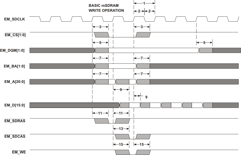 Figure 5-22 EMIF Basic SDRAM and mSDRAM Write Operation
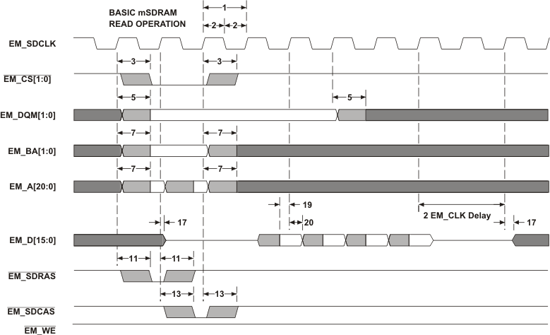 Figure 5-23 EMIF Basic SDRAM and mSDRAM Read Operation
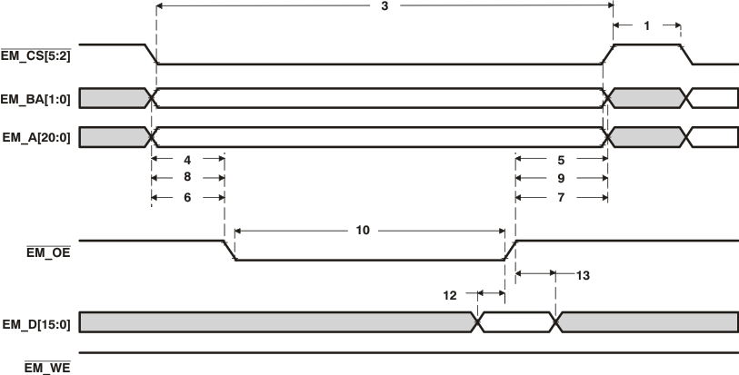 Figure 5-24 Asynchronous Memory Read Timing for EMIF
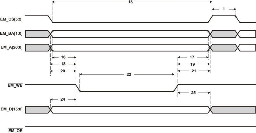 Figure 5-25 Asynchronous Memory Write Timing for EMIF
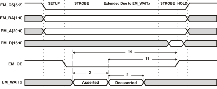 Figure 5-26 EM_WAITx Read Timing Requirements
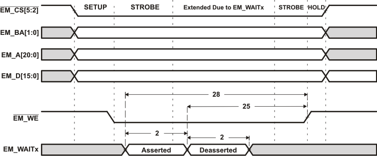 Figure 5-27 EM_WAITx Write Timing Requirements
5.7.7 General-Purpose Input/Output (GPIO)
The GPIO peripheral provides general-purpose pins that can be configured as either inputs or outputs. When configured as an output, you can write to an internal register to control the state driven on the output pin. When configured as an input, you can detect the state of the input by reading the state of the internal register. External input clocks on certain GPIOs can also be used to drive the timers on this device. The GPIO can also be used to send interrupts to the CPU.
The GPIO peripheral supports the following:
- Up to 26 GPIOs plus 1 general-purpose output (XF and 4 Special-Purpose Outputs for Use With SAR)
- The 26 GPIO pins have internal pulldowns (IPDs) which can be individually disabled
- The 26 GPIOs can be configured to generate edge detected interrupts to the CPU on either the rising or falling edge
The device GPIO pin functions are multiplexed with various other signals. For more detailed information on what signals are multiplexed with the GPIO and how to configure them, see Section 4.2, Signal Descriptions and Section 4.3, Pin Multiplexing of this document.
5.7.7.1 GPIO Peripheral Input/Output Electrical Data and Timing
Table 5-29 Timing Requirements for GPIO Inputs(1) (see Figure 5-28)
| NO. | CVDD = 1.05 V CVDD = 1.3 V/1.4 V |
UNIT | ||||
|---|---|---|---|---|---|---|
| MIN | MAX | |||||
| 1 | tw(ACTIVE) | Pulse duration, GPIO input/external interrupt pulse active | 2C(1)(2) | ns | ||
| 2 | tw(INACTIVE) | Pulse duration, GPIO input/external interrupt pulse inactive | C(1)(2) | ns | ||
Table 5-30 Switching Characteristics Over Recommended Operating Conditions for GPIO Outputs
(see Figure 5-28)
| NO. | PARAMETER | CVDD = 1.05 V CVDD = 1.3 V/1.4 V |
UNIT | ||
|---|---|---|---|---|---|
| MIN | MAX | ||||
| 3 | tw(GPOH) | Pulse duration, GP[x] output high | 3C(1)(2) | ns | |
| 4 | tw(GPOL) | Pulse duration, GP[x] output low | 3C(1)(2) | ns | |
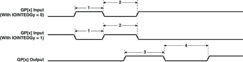 Figure 5-28 GPIO Port Timing
5.7.7.2 GPIO Peripheral Input Latency Electrical Data and Timing
Table 5-31 Timing Requirements for GPIO Input Latency(1)
| NO. | CVDD = 1.05 V CVDD = 1.3 V CVDD = 1.4 V |
UNIT | ||||
|---|---|---|---|---|---|---|
| MIN | MAX | |||||
| 1 | tL(GPI) | Latency, GP[x] input | Polling GPIO_DIN register | 5 | cyc | |
| Polling GPIO_IFR register | 7 | cyc | ||||
| Interrupt Detection | 8 | cyc | ||||
5.7.8 Inter-Integrated Circuit (I2C)
The inter-integrated circuit (I2C) module provides an interface between the device and other devices compliant with Philips Semiconductors Inter-IC bus (I2C-bus™) specification version 2.1. External components attached to this 2-wire serial bus can transmit and receive 2 to 8-bit data to and from the DSP through the I2C module. The I2C port does not support CBUS compatible devices.
The I2C port supports the following features:
- Compatible with Philips I2C Specification Version 2.1 (January 2000)
- Data Transfer Rate from 10 kbps to 400 kbps (Philips Fast-Mode Rate)
- Noise Filter to Remove Noise 50 ns or Less
- Seven- and Ten-Bit Device Addressing Modes
- Master (Transmit and Receive) and Slave (Transmit and Receive) Functionality
- One Read DMA Event and One Write DMA Event, which can be used by the DMA Controller
- One Interrupt that can be used by the CPU
- Slew-Rate Limited Open-Drain Output Buffers
The I2C module clock must be in the range from 6.7 MHz to 13.3 MHz. This is necessary for proper operation of the I2C module. With the I2C module clock in this range, the noise filters on the SDA and SCL pins suppress noise that has a duration of 50 ns or shorter. The I2C module clock is derived from the DSP clock divided by a programmable prescaler.
5.7.8.1 I2C Electrical Data and Timing
Table 5-32 Timing Requirements for I2C Timings(1) (see Figure 5-29)
| NO. | CVDD = 1.05 V CVDD = 1.3 V CVDD = 1.4 V |
UNIT | ||||||
|---|---|---|---|---|---|---|---|---|
| STANDARD MODE | FAST MODE | |||||||
| MIN | MAX | MIN | MAX | |||||
| 1 | tc(SCL) | Cycle time, SCL | 10 | 2.5 | µs | |||
| 2 | tsu(SCLH-SDAL) | Setup time, SCL high before SDA low (for a repeated START condition) | 4.7 | 0.6 | µs | |||
| 3 | th(SCLL-SDAL) | Hold time, SCL low after SDA low (for a START and a repeated START condition) | 4 | 0.6 | µs | |||
| 4 | tw(SCLL) | Pulse duration, SCL low | 4.7 | 1.3 | µs | |||
| 5 | tw(SCLH) | Pulse duration, SCL high | 4 | 0.6 | µs | |||
| 6 | tsu(SDAV-SCLH) | Setup time, SDA valid before SCL high | 250 | 100(2) | ns | |||
| 7 | th(SDA-SCLL) | Hold time, SDA valid after SCL low | 0(3) | 0(3) | 0.9(4) | µs | ||
| 8 | tw(SDAH) | Pulse duration, SDA high between STOP and START conditions | 4.7 | 1.3 | µs | |||
| 9 | tr(SDA) | Rise time, SDA(6) | 1000 | 20 + 0.1Cb(5) | 300 | ns | ||
| 10 | tr(SCL) | Rise time, SCL(6) | 1000 | 20 + 0.1Cb(5) | 300 | ns | ||
| 11 | tf(SDA) | Fall time, SDA(6) | 300 | 20 + 0.1Cb(5) | 300 | ns | ||
| 12 | tf(SCL) | Fall time, SCL(6) | 300 | 20 + 0.1Cb(5) | 300 | ns | ||
| 13 | tsu(SCLH-SDAH) | Setup time, SCL high before SDA high (for STOP condition) | 4 | 0.6 | µs | |||
| 14 | tw(SP) | Pulse duration, spike (must be suppressed) | 0 | 50 | ns | |||
| 15 | Cb(5) | Capacitive load for each bus line | 400 | 400 | pF | |||
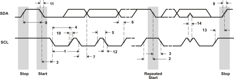 Figure 5-29 I2C Receive Timings
Table 5-33 Switching Characteristics for I2C Timings(1) (see Figure 5-30)
| NO. | PARAMETER | CVDD = 1.05 V CVDD = 1.3 V CVDD = 1.4 V |
UNIT | |||||
|---|---|---|---|---|---|---|---|---|
| STANDARD MODE | FAST MODE | |||||||
| MIN | MAX | MIN | MAX | |||||
| 16 | tc(SCL) | Cycle time, SCL | 10 | 2.5 | µs | |||
| 17 | td(SCLH-SDAL) | Delay time, SCL high to SDA low (for a repeated START condition) | 4.7 | 0.6 | µs | |||
| 18 | td(SDAL-SCLL) | Delay time, SDA low to SCL low (for a START and a repeated START condition) | 4 | 0.6 | µs | |||
| 19 | tw(SCLL) | Pulse duration, SCL low | 4.7 | 1.3 | µs | |||
| 20 | tw(SCLH) | Pulse duration, SCL high | 4 | 0.6 | µs | |||
| 21 | td(SDAV-SCLH) | Delay time, SDA valid to SCL high | 250 | 100 | ns | |||
| 22 | tv(SCLL-SDAV) | Valid time, SDA valid after SCL low | 0 | 0 | 0.9 | µs | ||
| 23 | tw(SDAH) | Pulse duration, SDA high between STOP and START conditions | 4.7 | 1.3 | µs | |||
| 24 | tr(SDA) | Rise time, SDA(2) | 1000 | 20 + 0.1Cb(1) | 300 | ns | ||
| 25 | tr(SCL) | Rise time, SCL(2) | 1000 | 20 + 0.1Cb(1) | 300 | ns | ||
| 26 | tf(SDA) | Fall time, SDA(2) | 300 | 20 + 0.1Cb(1) | 300 | ns | ||
| 27 | tf(SCL) | Fall time, SCL(2) | 300 | 20 + 0.1Cb(1) | 300 | ns | ||
| 28 | td(SCLH-SDAH) | Delay time, SCL high to SDA high (for STOP condition) | 4 | 0.6 | µs | |||
| 29 | Cp | Capacitance for each I2C pin | 10 | 10 | pF | |||
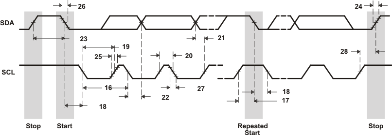 Figure 5-30 I2C Transmit Timings
5.7.9 Inter-IC Sound (I2S)
The device I2S peripherals allow serial transfer of full-duplex streaming data, usually audio data, between the device and an external I2S peripheral device such as an audio codec.
The device supports three independent dual-channel I2S peripherals, each with the following features:
- Full-duplex (transmit and receive) dual-channel communication
- Double buffered data registers that allow for continuous data streaming
- I2S/Left-justified and DSP data format with a data delay of 1 or 2 bits
- Data word-lengths of 8, 10, 12, 14, 16, 18, 20, 24, or 32 bits
- Ability to sign-extend received data samples for easy use in signal processing algorithms
- Programmable polarity for both frame synchronization and bit clocks
- Stereo (in I2S/Left-justified or DSP data formats) or mono (in DSP data format) mode
- Detection of over-run, under-run, and frame-sync error conditions
5.7.9.1 Inter-IC Sound (I2S) Electrical Data and Timing
Table 5-34 Timing Requirements for I2S [I/O = 3.3 and 2.75 V](1) (see Figure 5-31)
| NO. | MASTER | SLAVE | UNIT | ||||||||
|---|---|---|---|---|---|---|---|---|---|---|---|
| CVDD = 1.05 V | CVDD = 1.3/1.4 V | CVDD = 1.05 V | CVDD = 1.3/1.4 V | ||||||||
| MIN | MAX | MIN | MAX | MIN | MAX | MIN | MAX | ||||
| 1 | tc(CLK) | Cycle time, I2S_CLK | 2P(1)(2) | 2P(1)(2) | 2P(1)(2) | 2P(1)(2) | ns | ||||
| 2 | tw(CLKH) | Pulse duration, I2S_CLK high | P(1)(2) | P(1)(2) | P(1)(2) | P(1)(2) | ns | ||||
| 3 | tw(CLKL) | Pulse duration, I2S_CLK low | P(1)(2) | P(1)(2) | P(1)(2) | P(1)(2) | ns | ||||
| 7 | tsu(RXV-CLKH) | Setup time, I2S_RX valid before I2S CLK high (CLKPOL = 0) | 5 | 3 | 5 | 3 | ns | ||||
| tsu(RXV-CLKL) | Setup time, I2S_RX valid before I2S_CLK low (CLKPOL = 1) | 5 | 3 | 5 | 3 | ns | |||||
| 8 | th(CLKH-RXV) | Hold time, I2S_RX valid after I2S_CLK high (CLKPOL = 0) | 3 | 3 | 3 | 3 | ns | ||||
| th(CLKL-RXV) | Hold time, I2S_RX valid after I2S_CLK low (CLKPOL = 1) | 3 | 3 | 3 | 3 | ns | |||||
| 9 | tsu(FSV-CLKH) | Setup time, I2S_FS valid before I2S_CLK high (CLKPOL = 0) | – | – | 12.5 | 6.5 | ns | ||||
| tsu(FSV-CLKL) | Setup time, I2S_FS valid before I2S_CLK low (CLKPOL = 1) | – | – | 12.5 | 6.5 | ns | |||||
| 10 | th(CLKH-FSV) | Hold time, I2S_FS valid after I2S_CLK high (CLKPOL = 0) | – | – | tw(CLKH) + 0.7(3) | tw(CLKH) + 0.7(3) | ns | ||||
| th(CLKL-FSV) | Hold time, I2S_FS valid after I2S_CLK low (CLKPOL = 1) | – | – | tw(CLKL) + 0.7(3) | tw(CLKL) + 0.7(3) | ns | |||||
Table 5-35 Timing Requirements for I2S [I/O = 1.8 V](1) (see Figure 5-31)
| NO. | MASTER | SLAVE | UNIT | ||||||||
|---|---|---|---|---|---|---|---|---|---|---|---|
| CVDD = 1.05 V | CVDD = 1.3/1.4 V | CVDD = 1.05 V | CVDD = 1.3/1.4 V | ||||||||
| MIN | MAX | MIN | MAX | MIN | MAX | MIN | MAX | ||||
| 1 | tc(CLK) | Cycle time, I2S_CLK | 2P(1)(2) | 2P(1)(2) | 2P(1)(2) | 2P(1)(2) | ns | ||||
| 2 | tw(CLKH) | Pulse duration, I2S_CLK high | P(1)(2) | P(1)(2) | P(1)(2) | P(1)(2) | ns | ||||
| 3 | tw(CLKL) | Pulse duration, I2S_CLK low | P(1)(2) | P(1)(2) | P(1)(2) | P(1)(2) | ns | ||||
| 7 | tsu(RXV-CLKH) | Setup time, I2S_RX valid before I2S CLK high (CLKPOL = 0) | 5 | 3 | 5 | 3.5 | ns | ||||
| tsu(RXV-CLKL) | Setup time, I2S_RX valid before I2S_CLK low (CLKPOL = 1) | 5 | 3 | 5 | 3.5 | ns | |||||
| 8 | th(CLKH-RXV) | Hold time, I2S_RX valid after I2S_CLK high (CLKPOL = 0) | 3 | 3 | 3 | 3 | ns | ||||
| th(CLKL-RXV) | Hold time, I2S_RX valid after I2S_CLK low (CLKPOL = 1) | 3 | 3 | 3 | 3 | ns | |||||
| 9 | tsu(FSV-CLKH) | Setup time, I2S_FS valid before I2S_CLK high (CLKPOL = 0) | – | – | 12.5 | 15 | ns | ||||
| tsu(FSV-CLKL) | Setup time, I2S_FS valid before I2S_CLK low (CLKPOL = 1) | – | – | 12.5 | 15 | ns | |||||
| 10 | th(CLKH-FSV) | Hold time, I2S_FS valid after I2S_CLK high (CLKPOL = 0) | – | – | tw(CLKH) + 0.7(3) | tw(CLKH) + 0.71(3) | ns | ||||
| th(CLKL-FSV) | Hold time, I2S_FS valid after I2S_CLK low (CLKPOL = 1) | – | – | tw(CLKL) + 0.7(3) | tw(CLKL) + 0.71(3) | ns | |||||
Table 5-36 Switching Characteristics Over Recommended Operating Conditions for I2S Output
[I/O = 3.3 and 2.75 V] (see Figure 5-31)
| NO. | PARAMETER | MASTER | SLAVE | UNIT | ||||||||
|---|---|---|---|---|---|---|---|---|---|---|---|---|
| CVDD = 1.05 V | CVDD = 1.3/1.4 V | CVDD = 1.05 V | CVDD = 1.3/1.4 V | |||||||||
| MIN | MAX | MIN | MAX | MIN | MAX | MIN | MAX | |||||
| 1 | tc(CLK) | Cycle time, I2S_CLK | P(1)(2) | P(1)(2) | P(1)(2) | P(1)(2) | ns | |||||
| 2 | tw(CLKH) | Pulse duration, I2S_CLK high (CLKPOL = 0) | P(1)(2) | P(1)(2) | P(1)(2) | P(1)(2) | ns | |||||
| tw(CLKL) | Pulse duration, I2S_CLK low (CLKPOL = 1) | P(1)(2) | P(1)(2) | P(1)(2) | P(1)(2) | ns | ||||||
| 3 | tw(CLKL) | Pulse duration, I2S_CLK low (CLKPOL = 0) | P(1)(2) | P(1)(2) | P(1)(2) | P(1)(2) | ns | |||||
| tw(CLKH) | Pulse duration, I2S_CLK high (CLKPOL = 1) | P(1)(2) | P(1)(2) | P(1)(2) | P(1)(2) | ns | ||||||
| 4 | tdmax(CLKL-DXV) | Output Delay time, I2S_CLK low to I2S_DX valid (CLKPOL = 0) | 0 | 14.5 | 0 | 11 | 0 | 14.5 | 0 | 11 | ns | |
| tdmax(CLKH-DXV) | Output Delay time, I2S_CLK high to I2S_DX valid (CLKPOL = 1) | 0 | 14.5 | 0 | 11 | 0 | 14.5 | 0 | 11 | ns | ||
| 5 | tdmax(CLKL-FSV) | Delay time, I2S_CLK low to I2S_FS valid (CLKPOL = 0) | -2 | 7 | -1.74 | 5 | – | – | ns | |||
| tdmax(CLKH-FSV) | Delay time, I2S_CLK high to I2S_FS valid (CLKPOL = 1) | -2 | 7 | -1.74 | 5 | – | – | ns | ||||
Table 5-37 Switching Characteristics Over Recommended Operating Conditions for I2S Output
[I/O = 1.8 V] (see Figure 5-31)
| NO. | PARAMETER | MASTER | SLAVE | UNIT | ||||||||
|---|---|---|---|---|---|---|---|---|---|---|---|---|
| CVDD = 1.05 V | CVDD = 1.3/1.4 V | CVDD = 1.05 V | CVDD = 1.3/1.4 V | |||||||||
| MIN | MAX | MIN | MAX | MIN | MAX | MIN | MAX | |||||
| 1 | tc(CLK) | Cycle time, I2S_CLK | 50 or 2P(1)(2) | 40 or 2P(1)(2) | 50 or 2P(1)(2) | 40 or 2P(1)(2) | ns | |||||
| 2 | tw(CLKH) | Pulse duration, I2S_CLK high (CLKPOL = 0) | P(1)(2) | P(1)(2) | P(1)(2) | P(1)(2) | ns | |||||
| tw(CLKL) | Pulse duration, I2S_CLK low (CLKPOL = 1) | P(1)(2) | P(1)(2) | P(1)(2) | P(1)(2) | ns | ||||||
| 3 | tw(CLKL) | Pulse duration, I2S_CLK low (CLKPOL = 0) | P(1)(2) | P(1)(2) | P(1)(2) | P(1)(2) | ns | |||||
| tw(CLKH) | Pulse duration, I2S_CLK high (CLKPOL = 1) | P(1)(2) | P(1)(2) | P(1)(2) | P(1)(2) | ns | ||||||
| 4 | tdmax(CLKL-DXV) | Output Delay time, I2S_CLK low to I2S_DX valid (CLKPOL = 0) | 0 | 17.7 | 0 | 14.5 | 0 | 17.7 | 0 | 14.5 | ns | |
| tdmax(CLKH-DXV) | Output Delay time, I2S_CLK high to I2S_DX valid (CLKPOL = 1) | 0 | 17.7 | 0 | 14.5 | 0 | 17.7 | 0 | 14.5 | ns | ||
| 5 | tdmax(CLKL-FSV) | Delay time, I2S_CLK low to I2S_FS valid (CLKPOL = 0) | -2 | 7 | -2 | 5 | – | – | ns | |||
| tdmax(CLKH-FSV) | Delay time, I2S_CLK high to I2S_FS valid (CLKPOL = 1) | -2 | 7 | -2 | 5 | – | – | ns | ||||
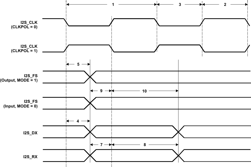 Figure 5-31 I2S Input and Output Timings
5.7.10 Multichannel Serial Port Interface (McSPI)
The multichannel SPI (McSPI) is a master and slave synchronous serial bus. McSPI allows a duplex, synchronous, serial communication to SPI-compliant external devices (slaves and masters).
The McSPI instances include the following main features:
- Serial clock with programmable frequency, polarity, and phase for each channel
- Wide selection of SPI word lengths ranging from 4 to 32 bits
- Up to three master channels or single channel in slave mode
- Master multichannel mode:
- Full duplex and half duplex
- Transmit-only and receive-only and transmit-and-receive modes
- Flexible I/O port controls per channel
- Two direct memory access (DMA) requests (read and write) per channel
- Single interrupt line for multiple interrupt source events
- Power management through wake-up capabilities
- Enable the addition of a programmable start-bit for SPI transfer per channel (start-bit mode)
- Support start-bit write command
- 128-bytes built-in FIFO available for a single channel
- Force CS mode for continuous transfers
5.7.10.1 McSPI Electrical Data and Timing
The multichannel SPI is a master and slave synchronous serial bus.
The following tables assume testing over the recommended operating conditions.
5.7.10.1.1 McSPI in Slave Mode
Table 5-38 McSPI Interface Timing Requirements – Slave Mode
| NO. | CVDD = 1.05 V | CVDD = 1.3/1.4 V | UNIT | ||||
|---|---|---|---|---|---|---|---|
| MIN | MAX | MIN | MAX | ||||
| SS2 | tsu(SIMOV-CLKAE) | Setup time, McSPI_SIMO valid before McSPI_CLK active edge | 4 | 3 | ns | ||
| SS3 | th(SIMOV-CLKAE) | Hold time, McSPI_SIMO valid after McSPI_CLK active edge | 3.8 | 2.8 | ns | ||
| SS4 | tsu(CS0V-CLKFE) | Setup time, McSPI_CS0 valid before McSPI_CLK first edge | 6.9 | 6.9 | ns | ||
| SS5 | th(CS0I-CLKLE) | Hold time, McSPI_CS0 invalid after McSPI_CLK last edge | 6.9 | 6.9 | ns | ||
Table 5-39 McSPI Interface Switching Characteristics — Slave Mode [I/O = 3.3 V]
| NO. | PARAMETER | CVDD = 1.05 V | CVDD = 1.3/1.4 V | UNIT | ||||
|---|---|---|---|---|---|---|---|---|
| MIN | MAX | MIN | MAX | |||||
| SS0 | Clock period | 14 | 22 | MHz | ||||
| SS1 | tw(CLK) | Pulse duration, McSPI_CLK high or low | 0.45*P(1) | 0.55*P(1) | 0.45*P(1) | 0.55*P(1) | ns | |
| SS6 | Output Delay time, McSPI_CLK active edge to McSPI_SOMI valid | 0 | 31 | 0 | 19 | ns | ||
| SS7 | Delay time, McSPI_CSn active edge to McSPIn_SOMI shifted, Mode 0 | 15 | 8.7 | ns | ||||
| SS7 | Delay time, McSPI_CSn active edge to McSPIn_SOMI shifted, Mode 2 | 15 | 8.7 | ns | ||||
Table 5-40 McSPI Interface Switching Characteristics — Slave Mode [I/O = 2.75 V]
| NO. | PARAMETER | CVDD = 1.05 V | CVDD = 1.3/1.4 V | UNIT | ||||
|---|---|---|---|---|---|---|---|---|
| MIN | MAX | MIN | MAX | |||||
| SS0 | Clock period | 12 | 19 | MHz | ||||
| SS1 | tw(CLK) | Pulse duration, McSPI_CLK high or low | 0.45*P(1) | 0.55*P(1) | 0.45*P(1) | 0.55*P(1) | ns | |
| SS6 | Output Delay time, McSPI_CLK active edge to McSPI_SOMI valid | 0 | 36 | 0 | 22.5 | ns | ||
| SS7 | Delay time, McSPI_CSn active edge to McSPIn_SOMI shifted | Modes 0 and 2 | 15 | 12 | ns | |||
Table 5-41 McSPI Interface Switching Characteristics — Slave Mode [I/O = 1.8 V]
| NO. | PARAMETER | CVDD = 1.05 V | CVDD = 1.3/1.4 V | UNIT | ||||
|---|---|---|---|---|---|---|---|---|
| MIN | MAX | MIN | MAX | |||||
| SS0 | Clock period | 12 | 18 | MHz | ||||
| SS1 | tw(CLK) | Pulse duration, McSPI_CLK high or low | 0.45*P(1) | 0.55*P(1) | 0.45*P(1) | 0.55*P(1) | ns | |
| SS6 | Output Delay time, McSPI_CLK active edge to McSPI_SOMI valid | 0 | 36 | 0 | 24 | ns | ||
| SS7 | Delay time, McSPI_CSn active edge to McSPIn_SOMI shifted | Modes 0 and 2 | 17 | 15 | ns | |||
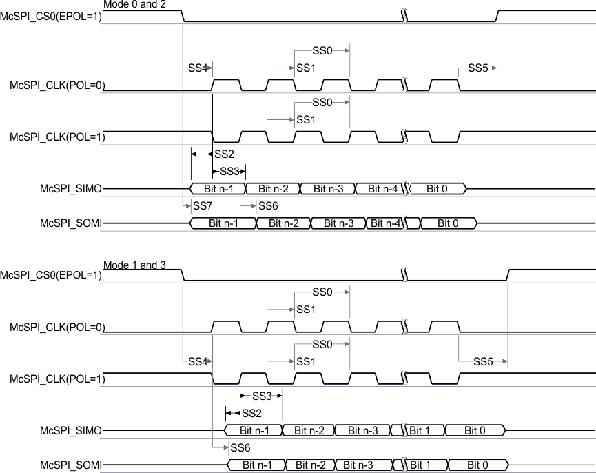 McSPI Interface — Transmit and Receive in Slave Mode
5.7.10.1.2 McSPI in Master Mode
The following tables assume testing over the recommended operating conditions (see ).
Table 5-42 McSPI Interface Timing Requirements – Master Mode [I/O = 3.3, 2.75 V]
| NO. | CVDD = 1.05 V | CVDD = 1.3/1.4 V | UNIT | ||||
|---|---|---|---|---|---|---|---|
| MIN | MAX | MIN | MAX | ||||
| SM2 | Setup time, McSPI_SOMI valid before McSPI_CLK active edge | 4 | 3 | ns | |||
| SM3 | Hold time, McSPI_SOMI valid after McSPI_CLK active edge | 3.8 | 2.8 | ns | |||
Table 5-43 McSPI Interface Timing Requirements – Master Mode [I/O = 1.8 V]
| NO. | CVDD = 1.05 V | CVDD = 1.3/1.4 V | UNIT | ||||
|---|---|---|---|---|---|---|---|
| MIN | MAX | MIN | MAX | ||||
| SM2 | Setup time, McSPI_SOMI valid before McSPI_CLK active edge | 7.5 | 3 | ns | |||
| SM3 | Hold time, McSPI_SOMI valid after McSPI_CLK active edge | 3.8 | 2.8 | ns | |||
Table 5-44 McSPI Interface Switching Characteristics – Master Mode [I/O = 3.3 V]
| NO. | PARAMETER | CVDD = 1.05 V | CVDD = 1.3/1.4 V | UNIT | ||||
|---|---|---|---|---|---|---|---|---|
| MIN | MAX | MIN | MAX | |||||
| SM0 | Clock period | 22 | 42 | MHz | ||||
| SM1 | Pulse duration, McSPI_CLK high or low | 0.45*P(1) | 0.55*P(1) | 0.45*P(1) | 0.55*P(1) | ns | ||
| SM4 | Delay time, McSPI_CLK active edge to McSPI_SIMO valid | 0 | 18 | -1 | 8.9 | ns | ||
| SM5 | Delay time, McSPI_CSx active to McSPI_CLK first edge | Modes 0–3 | 3.1 | 3.1 | ns | |||
| SM6 | Delay time, McSPI_CLK last edge to McSPI_CSx inactive | Modes 0–3 | 3.1 | 3.1 | ns | |||
| SM7 | Delay time, McSPI_CSx active edge to McSPI_SIMO shifted | Modes 0 and 2 | 10 | 6 | ns | |||
Table 5-45 McSPI Interface Switching Characteristics – Master Mode [I/O = 2.75 V]
| NO. | PARAMETER | CVDD = 1.05 V | CVDD = 1.3/1.4 V | UNIT | ||||
|---|---|---|---|---|---|---|---|---|
| MIN | MAX | MIN | MAX | |||||
| SM0 | Clock period | 22 | 38 | MHz | ||||
| SM1 | Pulse duration, McSPI_CLK high or low | 0.45*P(1) | 0.55*P(1) | 0.45*P(1) | 0.55*P(1) | ns | ||
| SM4 | Delay time, McSPI_CLK active edge to McSPI_SIMO valid | 0 | 18 | -1 | 10 | ns | ||
| SM5 | Delay time, McSPI_CSx active to McSPI_CLK first edge | Modes 0–3 | 3.1 | 3.1 | ns | |||
| SM6 | Delay time, McSPI_CLK last edge to McSPI_CSx inactive | Modes 0–3 | 3.1 | 3.1 | ns | |||
| SM7 | Delay time, McSPI_CSx active edge to McSPI_SIMO shifted | Modes 0 and 2 | 10 | 6 | ns | |||
Table 5-46 McSPI Interface Switching Characteristics – Master Mode [I/O = 1.8 V]
| NO. | PARAMETER | CVDD = 1.05 V | CVDD = 1.3/1.4 V | UNIT | ||||
|---|---|---|---|---|---|---|---|---|
| MIN | MAX | MIN | MAX | |||||
| SM0 | Clock period | 19 | 38 | MHz | ||||
| SM1 | Pulse duration, McSPI_CLK high or low | 0.45*P(1) | 0.55*P(1) | 0.45*P(1) | 0.55*P(1) | ns | ||
| SM4 | Delay time, McSPI_CLK active edge to McSPI_SIMO valid | 0 | 18.5 | -1 | 10 | ns | ||
| SM5 | Delay time, McSPI_CSx active to McSPI_CLK first edge | Modes 0–3 | 2.75 | 3 | ns | |||
| SM6 | Delay time, McSPI_CLK last edge to McSPI_CSx inactive | Modes 0–3 | 2.75 | 3 | ns | |||
| SM7 | Delay time, McSPI_CSx active edge to McSPI_SIMO shifted | Modes 0 and 2 | 11 | 5 | ns | |||
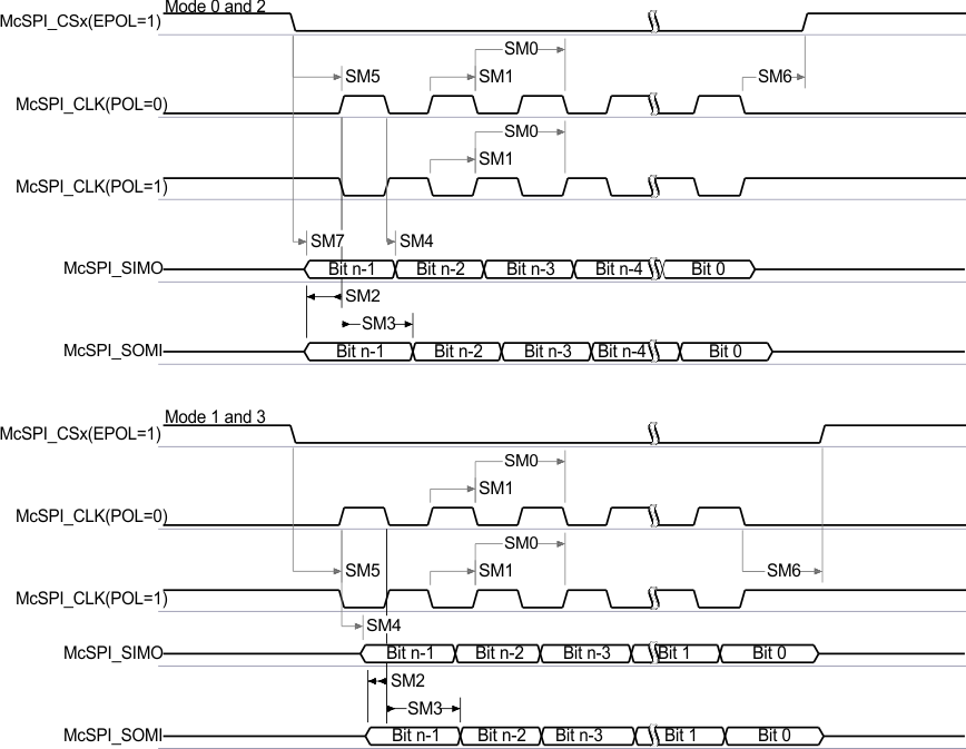 McSPI Interface — Transmit and Receive in Master Mode
5.7.11 Multichannel Buffered Serial Port (McBSP)
The McBSP provides these functions:
- Full-duplex communication
- Double-buffered data registers, which allow a continuous data stream
- Independent framing and clocking for receive and transmit
- Direct interface to industry-standard codecs, analog interface chips (AICs), and other serially connected analog-to-digital (A/D) and digital-to-analog (D/A) devices
- External shift clock or an internal, programmable frequency shift clock for data transfer
- Transmit and Receive FIFO Buffers allow the McBSP to operate at a higher sample rate by making it more tolerant to DMA latency
If the internal clock is used, the CLKGDV field of the Sample Rate Generator Register (SRGR) must always be set to a value of 3 or greater.
5.7.11.1 McBSP Electrical Data and Timing
Table 5-47 Timing Requirements for McBSP, DVDDIO 1.8 V (see )
| NO. | CVDD = 1.05 V | CVDD = 1.3/1.4 V | UNIT | |||||
|---|---|---|---|---|---|---|---|---|
| DVDDIO 1.8 V | ||||||||
| MIN | MAX | MIN | MAX | |||||
| 2 | tc(CKRX) | Cycle time, CLKR/X | CLKR/X ext | 15 | 9 | ns | ||
| 3 | tw(CKRX) | Pulse duration, CLKR/X high or CLKR/X low | CLKR/X ext | P-1(1) | P-1(1) | ns | ||
| 5 | tsu(FRH-CKRL) | Setup time, external FSR high before CLKR low | CLKR int | 29.5 | 29.5 | ns | ||
| CLKR ext | 3.5 | 3.5 | ||||||
| 6 | th(CKRL-FRH) | Hold time, external FSR high after CLKR low | CLKR int | 4.5 | 4.5 | ns | ||
| CLKR ext | 4.5 | 4.5 | ||||||
| 7 | tsu(DRV-CKRL) | Setup time, DR valid before CLKR low | CLKR int | 18.5 | 18.5 | ns | ||
| CLKR ext | 2.5 | 2.5 | ||||||
| 8 | th(CKRL-DRV) | Hold time, DR valid after CLKR low | CLKR int | -4 | -4 | ns | ||
| CLKR ext | 5.5 | 5.5 | ||||||
| 10 | tsu(FXH-CKXL) | Setup time, external FSX high before CLKX low | CLKX int | 26.5 | 26.5 | ns | ||
| CLKX ext | 7.5 | 7.5 | ||||||
| 11 | th(CKXL-FXH) | Hold time, external FSX high after CLKX low | CLKX int | 0.5 | 0.5 | ns | ||
| CLKX ext | 2.5 | 2.5 | ||||||
Table 5-48 Timing Requirements for McBSP,
DVDDIO 3.3/2.75 V (see )
| NO. | CVDD = 1.05 V | CVDD = 1.3/1.4 V | UNIT | |||||
|---|---|---|---|---|---|---|---|---|
| DVDDIO 3.3/2.75 V | ||||||||
| MIN | MAX | MIN | MAX | |||||
| 2 | tc(CKRX) | Cycle time, CLKR/X | CLKR/X ext | 18 | 9 | ns | ||
| 3 | tw(CKRX) | Pulse duration, CLKR/X high or CLKR/X low | CLKR/X ext | P-1(1) | P-1(1) | ns | ||
| 5 | tsu(FRH-CKRL) | Setup time, external FSR high before CLKR low | CLKR int | 24 | 24 | ns | ||
| CLKR ext | 4 | 4 | ||||||
| 6 | th(CKRL-FRH) | Hold time, external FSR high after CLKR low | CLKR int | 4 | 4 | ns | ||
| CLKR ext | 5 | 5 | ||||||
| 7 | tsu(DRV-CKRL) | Setup time, DR valid before CLKR low | CLKR int | 22.5 | 22.5 | ns | ||
| CLKR ext | 2.5 | 2.5 | ||||||
| 8 | th(CKRL-DRV) | Hold time, DR valid after CLKR low | CLKR int | -3 | -3 | ns | ||
| CLKR ext | 6 | 6 | ||||||
| 10 | tsu(FXH-CKXL) | Setup time, external FSX high before CLKX low | CLKX int | 23 | 23 | ns | ||
| CLKX ext | 7 | 7 | ||||||
| 11 | th(CKXL-FXH) | Hold time, external FSX high after CLKX low | CLKX int | 2 | 2 | ns | ||
| CLKX ext | 3 | 3 | ||||||
Table 5-49 Switching Characteristics Over Recommended Operating Conditions for McBSP,
DVDDIO 1.8 V
(see )
| NO. | PARAMETER | CVDD = 1.05 V | CVDD = 1.3/1.4 V | UNIT | ||||
|---|---|---|---|---|---|---|---|---|
| DVDDIO 1.8 V | ||||||||
| MIN | MAX | MIN | MAX | |||||
| 1 | td(CKSH-CKRXH) | Delay time, CLKS high to CLKR/X high for internal CLKR/X generated from CLKS input | 5.5 | 25 | 5.5 | 25 | ns | |
| 2 | tc(CKRX) | Cycle time, CLKR/X | CLKR/X int | 15 | 9 | ns | ||
| 3 | tw(CKRX) | Pulse duration, CLKR/X high or CLKR/X low | CLKR/X int | C+2(1) | C+2(1) | ns | ||
| 4 | td(CKRH-FRV) | Delay time, CLKR high to internal FSR valid | CLKR int | -6.5 | 6 | -6.5 | 6 | ns |
| 9 | td(CKXH-FXV) | Delay time, CLKX high to internal FSX valid | CLKX int | -2 | 1 | -2 | 1 | ns |
| CLKX ext | 4 | 23 | 4 | 23 | ||||
| 12 | tdis(CKXH-DXHZ) | Disable time, DX high impedance following last data bit from CLKX high | CLKX int | -5 | 3 | -5 | 3 | ns |
| CLKX ext | 3 | 24.5 | 3 | 24.5 | ||||
| 13 | td(CKXH-DXV) | Delay time, CLKX high to DX valid | CLKX int | -4.5 | 4 | -4.5 | 4 | ns |
| CLKX ext | 3.5 | 25.5 | 3.5 | 25.5 | ||||
| 14 | td(FXH-DXV) | Delay time, FSX high to DX valid |
FSX int | -4 | 4 | -4 | 4 | ns |
| ONLY applies when in data delay 0 (XDATDLY = 00b) mode |
FSX ext | -2 | 3 | -2 | 3 | |||
S = sample rate generator input clock = P if CLKSM = 1 (P = SYSCLK period)
S = sample rate generator input clock = P_clks if CLKSM = 0 (P_clks = CLKS period)
H = CLKX high pulse duration = (CLKGDV/2 + 1) * S if CLKGDV is even
H = (CLKGDV + 1)/2 * S if CLKGDV is odd
L = CLKX low pulse duration = (CLKGDV/2) * S if CLKGDV is even
L = (CLKGDV + 1)/2 * S if CLKGDV is odd
CLKGDV should be set appropriately to ensure the McBSP bit rate does not exceed the maximum limit (see (4) above).
Table 5-50 Switching Characteristics Over Recommended Operating Conditions for McBSP,
DVDDIO 3.3/2.75 V
(see )
| NO. | PARAMETER | CVDD = 1.05 V | CVDD = 1.3/1.4 V | UNIT | ||||
|---|---|---|---|---|---|---|---|---|
| DVDDIO 3.3/2.75 V | ||||||||
| MIN | MAX | MIN | MAX | |||||
| 1 | td(CKSH-CKRXH) | Delay time, CLKS high to CLKR/X high for internal CLKR/X generated from CLKS input | 4.25 | 24 | 4.5 | 24 | ns | |
| 2 | tc(CKRX) | Cycle time, CLKR/X | CLKR/X int | 18 | 9 | ns | ||
| 3 | tw(CKRX) | Pulse duration, CLKR/X high or CLKR/X low | CLKR/X int | C-2(1) | C-2(1) | ns | ||
| 4 | td(CKRH-FRV) | Delay time, CLKR high to internal FSR valid | CLKR int | -4 | 8 | -4 | 8 | ns |
| 9 | td(CKXH-FXV) | Delay time, CLKX high to internal FSX valid | CLKX int | -2 | 2 | -2 | 2 | ns |
| CLKX ext | 3.5 | 20 | 3.5 | 20 | ||||
| 12 | tdis(CKXH-DXHZ) | Disable time, DX high impedance following last data bit from CLKX high | CLKX int | -2.5 | 4 | -2.5 | 4 | ns |
| CLKX ext | 3 | 21 | -3 | 21 | ||||
| 13 | td(CKXH-DXV) | Delay time, CLKX high to DX valid | CLKX int | -2.5 | 5 | -2.5 | 5 | ns |
| CLKX ext | 3 | 22.5 | 3 | 22.5 | ||||
| 14 | td(FXH-DXV) | Delay time, FSX high to DX valid |
FSX int | -1.5 | 4 | -1.5 | 4 | ns |
| ONLY applies when in data delay 0 (XDATDLY = 00b) mode |
FSX ext | -1.5 | 3.5 | -1.5 | 3.5 | |||
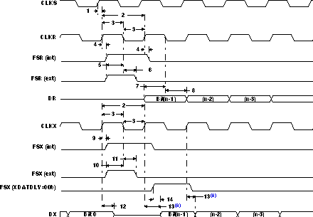
Table 5-51 Timing Requirements for FSR When GSYNC = 1 (see )
| NO. | CVDD = 1.05 V | CVDD = 1.3/1.4 V | UNIT | ||||
|---|---|---|---|---|---|---|---|
| DVDDIO 3.3/2.75/1.8 V | |||||||
| MIN | MAX | MIN | MAX | ||||
| 1 | tsu(FRH-CKSH) | Setup time, FSR high before CLKS high | 5 | 5 | ns | ||
| 2 | th(CKSH-FRH) | Hold time, FSR high after CLKS high | 4 | 4 | ns | ||
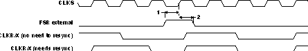 FSR Timing When GSYNC = 1
5.7.12 Multimedia Card and Secure Digital (eMMC, MMC, SD, and SDHC)
The device includes two MMC and SD controllers which are compliant with eMMC V4.3, MMC V3.31, Secure Digital Part 1 Physical Layer Specification V2.0, and Secure Digital Input Output (SDIO) V2.0 specifications. The MMC and SD card controller supports these industry standards and assumes the reader is familiar with these standards.
Each MMC and SD Controller in the device has the following features:
- Multimedia Card and Secure Digital (eMMC, MMC, SD, and SDHC) protocol support
- Programmable clock frequency
- 256-bit Read and Write FIFO to lower system overhead
- Slave DMA transfer capability
The MMC and SD card controller transfers data between the CPU and DMA controller on one side and MMC and SD card on the other side. The CPU and DMA controller can read and write the data in the card by accessing the registers in the MMC and SD controller.
The MMC and SD controller on this device, does not support the SPI mode of operation.
5.7.12.1 MMC and SD Electrical Data and Timing
Table 5-52 Timing Requirements for MMC and SD (see Figure 5-32 and Figure 5-35)
| NO. | CVDD = 1.3/1.4 V | CVDD = 1.05 V | UNIT | ||||
|---|---|---|---|---|---|---|---|
| FAST MODE | STD MODE | ||||||
| MIN | MAX | MIN | MAX | ||||
| 1 | tsu(CMDV-CLKH) | Setup time, MMCx_CMD data input valid before MMCx_CLK high | 3 | 3 | ns | ||
| 2 | th(CLKH-CMDV) | Hold time, MMCx_CMD data input valid after MMCx_CLK high | 3 | 3 | ns | ||
| 3 | tsu(DATV-CLKH) | Setup time, MMC_Dx data input valid before MMCx_CLK high | 3 | 3.1 | ns | ||
| 4 | th(CLKH-DATV) | Hold time, MMC_Dx data input valid after MMCx_CLK high | 3 | 3 | ns | ||
Table 5-53 Switching Characteristics Over Recommended Operating Conditions for MMC Output(2) (see Figure 5-32 and Figure 5-35)
| NO. | PARAMETER | CVDD = 1.3/1.4 V | CVDD = 1.05 V | UNIT | |||
|---|---|---|---|---|---|---|---|
| FAST MODE | STD MODE | ||||||
| MIN | MAX | MIN | MAX | ||||
| 7 | f(CLK) | Operating frequency, MMCx_CLK | 0 | 50(1) | 0 | 25(1) | MHz |
| 8 | f(CLK_ID) | Identification mode frequency, MMCx_CLK | 0 | 400 | 0 | 400 | kHz |
| 9 | tw(CLKL) | Pulse duration, MMCx_CLK low | 7 | 10 | ns | ||
| 10 | tw(CLKH) | Pulse duration, MMCx_CLK high | 7 | 10 | ns | ||
| 11 | tr(CLK) | Rise time, MMCx_CLK | 3 | 3 | ns | ||
| 12 | tf(CLK) | Fall time, MMCx_CLK | 3 | 3 | ns | ||
| 13 | td(MDCLKL-CMDIV) | Delay time, MMCx_CLK low to MMC_CMD data output invalid | -4.53 | -4.77 | ns | ||
| 14 | td(MDCLKL-CMDV) | Delay time, MMCx_CLK low to MMC_CMD data output valid | 4.1 | 5.4 | ns | ||
| 15 | td(MDCLKL-DATIV) | Delay time, MMCx_CLK low to MMC_Dx data output invalid | -4.53 | -4.77 | ns | ||
| 16 | td(MDCLKL-DATV) | Delay time, MMCx_CLK low to MMC_Dx data output valid | 4.1 | 5.4 | ns | ||
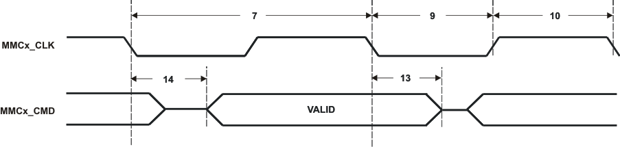 Figure 5-32 MMC and SD Host Command Write Timing
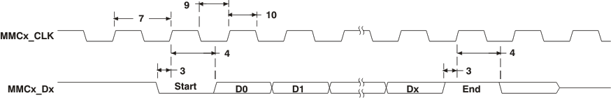 Figure 5-33 MMC and SD Card Response Timing
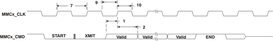 Figure 5-34 MMC and SD Host Write Timing
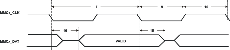 Figure 5-35 MMC and SD Data Write Timing
5.7.13 Real-Time Clock (RTC)
The device includes a Real-Time Clock (RTC) with its own separate power supply and isolation circuits. The RTC has the capability to wake up the device from idle states via alarms, periodic interrupts, or an external WAKEUP input.
To prevent unintentional access to the RTC registers, gate-keeper registers must be programmed with a specific signature—0x95A4_F1E0—before changing the RTC registers.
Note: The RTC Core (CVDDRTC) must be powered by an external power source even though RTC is not used. None of the on-chip LDOs can power CVDDRTC.
The device RTC provides the following features:
- 100-year calendar up to year 2099.
- Counts milliseconds, seconds, minutes, hours, day of the week, date, month, and year with leap year compensation
- Millisecond time correction
- Binary-coded-decimal (BCD) representation of time, calendar, and alarm
- 24-hour clock mode
- Second, minute, hour, or day alarm interrupt
- Periodic interrupt: every millisecond, second, minute, hour, or day
- Alarm interrupt: precise time of day
- Single interrupt to the DSP CPU
- 32.768-kHz crystal oscillator with frequency calibration
- Bidirectional IO pin that can be set up as:
- Input for an external device to wake up the DSP
- Output to wake up an external device
Control of the RTC is maintained through a set of I/O memory mapped registers (see Table 6-19). Note that any write to these registers will be synchronized to the RTC 32.768-kHz clock; thus, the CPU must run at least 3X faster than the RTC. Writes to these registers will not be evident until the next two 32.768-kHz clock cycles later.
Furthermore, three conditions must be met to write to the RTC registers:
- The RTC oscillator must be enabled.
- A 1 must be written to the RTC system control register (RSCR) to bring the RTC out of isolation.
- The gate-keeper registers (RGKR_LSW and RGKR_MSW) must contain the key 0x95A4_F1E0.
If these conditions are not met, the RTC remains isolated and protected from power glitches.
For more information, see the Static Power Management section of the TMS320C5517 Digital Signal Processor Technical Reference Manual [literature number SPRUH16].
The RTC has its own power-on-reset (POR) circuit which resets the registers in the RTC core domain when power is first applied to the CVDDRTC power pin. The RTC flops are not reset by the device's RESET pin nor the digital core's POR (powergood signal).
The scratch registers in the RTC can be used to take advantage of this unique reset domain to keep track of when the DSP boots and whether the RTC time registers have already been initialized to the current clock time or whether the software needs to go into a routine to prompt the user to set the time and date.
5.7.13.1 RTC Electrical Data and Timing
For more detailed information on RTC electrical timings, specifically WAKEUP, see Section 5.7.3.3, Reset Electrical Data and Timing.
5.7.14 SAR ADC (10-Bit)
The device includes a 10-bit SAR ADC using a switched capacitor architecture which converts an analog input signal to a digital value at a maximum rate of 62.5-k samples per second (ksps) for use by the DSP. This SAR module supports six channels that are connected to four general purpose analog pins (GPAIN [3:0]) which can be used as general purpose outputs.
The device SAR supports the following features:
- Up to 62.5 ksps (2-MHz clock with 32 cycles per conversion)
- Single conversion and continuous back-to-back conversion modes
- Interrupt driven or polling conversion or DMA event generation
- Internal configurable bandgap reference voltages of 1 V or 0.8 V; or external Vref of VDDA_ANA
- One 3.6-V Tolerant analog input (GPAIN0) with internal voltage division for conversion of battery voltage
- Software controlled power down
- Individually configurable general-purpose digital outputs
5.7.14.1 SAR ADC Electrical Data and Timing
Table 5-54 Switching Characteristics Over Recommended Operating Conditions for ADC Characteristics
| NO. | PARAMETER | CVDD = 1.4 V CVDD = 1.3 V CVDD = 1.05 V |
UNIT | |||
|---|---|---|---|---|---|---|
| MIN | TYP | MAX | ||||
| 1 | tC(SCLC) | Cycle time, ADC internal conversion clock | 2 | MHz | ||
| 3 | td(CONV) | Delay time, ADC conversion time | 32tC(SCLC) | ns | ||
| 4 | SDNL | Static differential non-linearity error (DNL measured for 9 bits) | ±0.6 | LSB | ||
| 5 | SINL | Static integral non-linearity error | ±1 | LSB | ||
| 6 | Zset | Zero-scale offset error (INL measured for 9 bits) | 2 | LSB | ||
| 7 | Fset | Full-scale offset error | 2 | LSB | ||
| 8 | Analog input impedance | 1 | MΩ | |||
| 9 | Signal-to-noise ratio | 54 | dB | |||
5.7.15 Serial Port Interface (SPI)
The device serial port interface (SPI) is a high-speed synchronous serial input/output port that allows a serial bit stream of programmed length (1 to 32 bits) to be shifted into and out of the device at a programmed bit-transfer rate. The SPI supports multi-chip operation of up to four SPI slave devices. The SPI can operate as a master device only, slave mode is not supported.Note: The SPI is not supported by the device DMA controller, so DMA cannot be used in transferring data between the SPI and the on-chip RAM.
The SPI is normally used for communication between the DSP and external peripherals. Typical applications include an interface to external I/O or peripheral expansion via devices such as shift registers, display drivers, SPI EEPROMs, and analog-to-digital converters.
The SPI has the following features:
- Programmable divider for serial data clock generation
- Four pin interface (SPI_CLK, SPI_CSn, SPI_RX, and SPI_TX)
- Programmable data length (1 to 32 bits)
- 4 external chip select signals
- Programmable transfer or frame size (1 to 4096 characters)
- Optional interrupt generation on character completion
- Optional interrupt generation on frame completion
- Programmable SPI_CSn to SPI_TX delay from 0 to 3 SPI_CLK cycles
- Programmable signal polarities
- Programmable active clock edge
- Internal loopback mode for testing
5.7.15.1 SPI Electrical Data and Timing
Table 5-55 Timing Requirements for SPI Inputs (see Figure 5-36 through Figure 5-39)
| NO. | CVDD = 1.05 V | CVDD = 1.3/1.4 V | UNIT | |||||
|---|---|---|---|---|---|---|---|---|
| MIN | MAX | MIN | MAX | |||||
| 4 | tC(SCLK) | Cycle time, SPI_CLK | 4P(1)(2) | 4P(1)(2) | ns | |||
| 5 | tw(SCLKH) | Pulse duration, SPI_CLK high | 30 | 19 | ns | |||
| 6 | tw(SCLKL) | Pulse duration, SPI_CLK low | 30 | 19 | ns | |||
| 7 | tsu(SRXV-SCLK) | Setup time, SPI_RX valid before SPI_CLK high | Modes 0, 2, and 3 | 16.1 | 13.9 | ns | ||
| Setup time, SPI_RX valid before SPI_CLK low | Mode 1 | 16.1 | 13.9 | ns | ||||
| 8 | th(SCLK-SRXV) | Hold time, SPI_RX valid after SPI_CLK high | Modes 0 and 3 | 0 | 0 | ns | ||
| Hold time, SPI_RX valid after SPI_CLK low | Modes 1 and 2 | 0 | 0 | ns | ||||
Table 5-56 Switching Characteristics Over Recommended Operating Conditions for SPI Outputs [I/O = 2.75 and 3.3 V]
(see Figure 5-36 through Figure 5-39)
| NO. | PARAMETER | CVDD = 1.05 V | CVDD = 1.3/1.4 V | UNIT | ||||
|---|---|---|---|---|---|---|---|---|
| MIN | MAX | MIN | MAX | |||||
| 1 | td(SCLK-STXV) | Delay time, SPI_CLK low to SPI_TX valid | Modes 0 and 3 | -4.2 | 8.9 | -4.9 | 5.3 | ns |
| Delay time, SPI_CLK high to SPI_TX valid | Modes 1 and 2 | -4.2 | 8.9 | -4.9 | 5.3 | ns | ||
| 2 | td(SPICS-SCLK) | Delay time, SPI_CS active to SPI_CLK active | tc - 8 + D(1) | tc - 8 + D(1) | ns | |||
| 3 | toh(SCLKI-SPICSI) | Output hold time, SPI_CS inactive to SPI_CLK inactive | 0.5tc - 1.9 | 0.5tc - 1.9 | ns | |||
Table 5-57 Switching Characteristics Over Recommended Operating Conditions for SPI Outputs [I/O = 1.8 V]
(see Figure 5-36 through Figure 5-39)
| NO. | PARAMETER | CVDD = 1.05 V | CVDD = 1.3/1.4 V | UNIT | ||||
|---|---|---|---|---|---|---|---|---|
| MIN | MAX | MIN | MAX | |||||
| 1 | td(SCLK-STXV) | Delay time, SPI_CLK low to SPI_TX valid | Modes 0 and 3 | -6.7 | 8.9 | -6.7 | 5.8 | ns |
| Delay time, SPI_CLK high to SPI_TX valid | Modes 1 and 2 | -6.7 | 8.9 | -6.7 | 5.8 | ns | ||
| 2 | td(SPICS-SCLK) | Delay time, SPI_CS active to SPI_CLK active | tc - 9.2 + D(1) | tc - 8 + D(1) | ns | |||
| 3 | toh(SCLKI-SPICSI) | Output hold time, SPI_CS inactive to SPI_CLK inactive | 0.5tc - 1.9 | 0.5tc - 1.9 | ns | |||
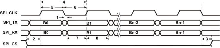
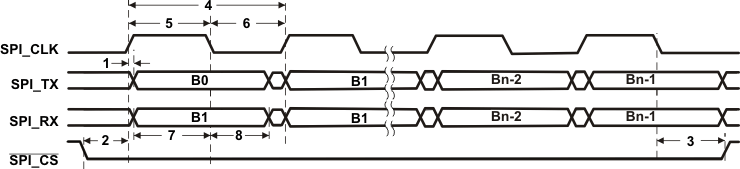
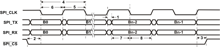
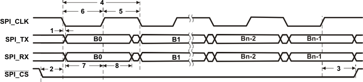
5.7.16 Timers
The device has three 32-bit software programmable Timers. Each timer can be used as a general- purpose (GP) timer. Timer2 can be configured as either a GP or a Watchdog (WD) or both. General-purpose timers are typically used to provide interrupts to the CPU to schedule periodic tasks or a delayed task. A watchdog timer is used to reset the CPU in case it gets into an infinite loop. The GP timers are 32-bit timers with a 13-bit prescaler that can divide the CPU clock and uses this scaled value as a reference clock. These timers can be used to generate periodic interrupts. The Watchdog Timer is a 16-bit counter with a 16-bit prescaler used to provide a recovery mechanism for the device in the event of a fault condition, such as a non-exiting code loop.
The device Timers support the following:
- 32-bit Programmable Countdown Timer
- 13-bit Prescaler Divider
- Timer Modes:
- 32-bit General-Purpose Timer
- 32-bit Watchdog Timer (Timer2 only)
- Auto Reload Option
- Generates a single interrupt to the CPU, which can be configured as a timer interrupt (TINT) or as a non-maskable interrupt (NMI). The interrupt is individually latched to determine which timer triggered the interrupt.
- Generates an active low pulse to the hardware reset (Watchdog only)
- Interrupt can be used for DMA Event
5.7.17 Universal Asynchronous Receiver and Transmitter (UART)
The UART performs serial-to-parallel conversions on data received from an external peripheral device and parallel-to-serial conversions on data transmitted to an external peripheral device via a serial bus.
The device has one UART peripheral with the following features:
- Programmable baud rates (frequency pre-scale values from 1 to 65535)
- Fully programmable serial interface characteristics:
- 5, 6, 7, or 8-bit characters
- Even, odd, or no PARITY bit generation and detection
- 1, 1.5, or 2 STOP bit generation
- 16-byte depth transmitter and receiver FIFOs:
- The UART can be operated with or without the FIFOs
- 1, 4, 8, or 14 byte selectable receiver FIFO trigger level for autoflow control and DMA
- DMA signaling capability for both received and transmitted data
- CPU interrupt capability for both received and transmitted data
- False START bit detection
- Line break generation and detection
- Internal diagnostic capabilities:
- Loopback controls for communications link fault isolation
- Break, parity, overrun, and framing error simulation
- Programmable autoflow control using CTS and RTS signals
5.7.17.1 UART Electrical Data and Timing [Receive and Transmit]
Table 5-58 Timing Requirements for UART Receive(1)(2) (see Figure 5-40)
| NO. | CVDD = 1.05/1.3/1.4 V | UNIT | |||
|---|---|---|---|---|---|
| MIN | MAX | ||||
| 4 | tw(URXDB) | Pulse duration, receive data bit (UART_RXD) [15/30 pF] | U - 3.5 | U + 3 | ns |
| 5 | tw(URXSB) | Pulse duration, receive start bit [15/30 pF] | U - 3.5 | U + 3 | ns |
Table 5-59 Switching Characteristics Over Recommended Operating Conditions
for UART Transmit(1)(2)
(see Figure 5-40)
| NO. | PARAMETER | CVDD = 1.05/1.3/1.4V | UNIT | ||
|---|---|---|---|---|---|
| MIN | MAX | ||||
| 1 | f(baud) | Maximum programmable bit rate | fmax/16 | MHz | |
| 2 | tw(UTXDB) | Pulse duration, transmit data bit (UART_TXD) [15/30 pF] | U - 3.5 | U + 4 | ns |
| 3 | tw(UTXSB) | Pulse duration, transmit start bit [15/30 pF] | U - 3.5 | U + 4 | ns |
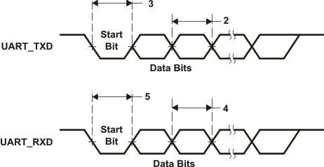 Figure 5-40 UART Transmit and Receive Timing
5.7.18 Universal Host-Port Interface (UHPI)
The device includes a user-configurable 16-bit universal host-port interface (UHPI16). The UHPI provides a parallel port interface through which an external host processor can directly access the processor's resources (configuration and program and data memories). The external host device is asynchronous to the CPU clock and functions as a master to the UHPI interface. The UHPI enables a host device and the processor to exchange information via internal memory. Dedicated address (UHPIA) and data (UHPID) registers within the UHPI provide the data path between the external host interface and the processor resources. A UHPI control register (UHPIC) is available to the host and the CPU for various configuration and interrupt functions.
5.7.18.1 UHPI Electrical Data and Timing
Table 5-60 Timing Requirements for Host-Port Interface, DVDDIO = 3.3/2.75 V
| NO. | DVDDIO = 3.3/2.75 V | UNIT | |||||
|---|---|---|---|---|---|---|---|
| CVDD = 1.05 V | CVDD = 1.3/1.4 V | ||||||
| MIN | MAX | MIN | MAX | ||||
| 1 | tsu(SELV-HSTBL) | Setup time, select signals(1) valid before HSTROBE low | 6.5 | 5 | ns | ||
| 2 | th(HSTBL-SELV) | Hold time, select signals(1) valid after HSTROBE low | 3 | 2 | ns | ||
| 3 | tw(HSTBL) | Pulse duration, HSTROBE active low | 19 | 17 | ns | ||
| 4 | tw(HSTBH) | Pulse duration, HSTROBE inactive high between consecutive accesses | 2P(2) | 2P(2) | ns | ||
| 11 | tsu(HDV-HSTBH) | Setup time, host data valid before HSTROBE high | 7.8 | 5 | ns | ||
| 12 | th(HSTBH-HDV) | Hold time, host data valid after HSTROBE high | 3.3 | 2.5 | ns | ||
| 13 | th(HRDYL-HSTBH) | Hold time, HSTROBE high after UHPI_HRDY high. HSTROBE should not be inactivated until UHPI_HRDY is active (high); otherwise, UHPI writes will not complete properly. | 2 | 2 | ns | ||
Table 5-61 Timing Requirements for Host-Port Interface, DVDDIO = 1.8 V
| NO. | DVDDIO = 1.8 V | UNIT | |||||
|---|---|---|---|---|---|---|---|
| CVDD = 1.05 V | CVDD = 1.3/1.4 V | ||||||
| MIN | MAX | MIN | MAX | ||||
| 1 | tsu(SELV-HSTBL) | Setup time, select signals(1) valid before HSTROBE low | 7.3 | 5 | ns | ||
| 2 | th(HSTBL-SELV) | Hold time, select signals(1) valid after HSTROBE low | 3 | 2 | ns | ||
| 3 | tw(HSTBL) | Pulse duration, HSTROBE active low | 24 | 19 | ns | ||
| 4 | tw(HSTBH) | Pulse duration, HSTROBE inactive high between consecutive accesses | 2P(2) | 2P(2) | ns | ||
| 11 | tsu(HDV-HSTBH) | Setup time, host data valid before HSTROBE high | 8.6 | 5 | ns | ||
| 12 | th(HSTBH-HDV) | Hold time, host data valid after HSTROBE high | 3.3 | 2.5 | ns | ||
| 13 | th(HRDYL-HSTBH) | Hold time, HSTROBE high after UHPI_HRDY high. HSTROBE should not be inactivated until UHPI_HRDY is active (high); otherwise, UHPI writes will not complete properly. | 2 | 2 | ns | ||
Table 5-62 Switching Characteristics Over Recommended Operating Conditions for Host-Port Interface, DVDDIO = 3.3/2.75 V
| NO. | PARAMETER | DVDDIO = 3.3/2.75 V | UNIT | |||||
|---|---|---|---|---|---|---|---|---|
| CVDD = 1.05 V | CVDD = 1.3/1.4 V | |||||||
| MIN | MAX | MIN | MAX | |||||
| 5 | td(HSTBL-HRDYV) | Delay time, HSTROBE low to UHPI_HRDY valid | For UHPI Write, UHPI_HRDY can go low (not ready) for these UHPI Write conditions; otherwise, UHPI_HRDY stays high (ready): Case 1: Back-to-back HPIA writes (can be either first or second half-word) Case 2: HPIA write following a PREFETCH command (can be either first or second half-word) Case 3: HPID write when FIFO is full or flushing (can be either first or second half-word) Case 4: HPIA write and Write FIFO not empty For UHPI Read, UHPI_HRDY can go low (not ready) for these UHPI Read conditions: Case 1: UHPID read (with auto-increment) and data not in Read FIFO (can only happen to first half-word of HPID access) Case 2: First half-word access of HPID Read without auto-increment For UHPI Read, UHPI_HRDY stays high (ready) for these UHPI Read conditions: Case 1: HPID read with auto-increment and data is already in Read FIFO (applies to either half-word of HPID access) Case 2: HPID read without auto-increment and data is already in Read FIFO (always applies to second half-word of HPID access) Case 3: HPIC or HPIA read (applies to either half-word access) |
0 | 22.3 | 0 | 15.5 | ns |
| 6 | ten(HSTBL-HDLZ) | Enable time, UHPI_HD driven from HSTROBE low | 1.5 | 1.5 | ns | |||
| 7 | td(HRDYL-HDV) | Delay time, UHPI_HRDY high to HD valid | 0 | 1.1 | ns | |||
| 8 | toh(HSTBH-HDV) | Output hold time, UHPI_HD valid after HSTROBE high | 1.5 | 1.5 | ns | |||
| 14 | tdis(HSTBH-HDHZ) | Disable time, HD high-impedance from HSTROBE high | 24.3 | 15.8 | ns | |||
| 15 | td(HSTBL-HDV) | Delay time, HSTROBE low to HD valid | For UHPI Read. Applies to conditions where data is already residing in HPID/FIFO: Case 1: HPIC or HPIA read Case 2: First half-word of HPID read with auto-increment and data is already in Read FIFO Case 3: Second half-word of HPID read with or without auto-increment |
24.3 | 15.8 | ns | ||
| 18 | td(HSTBH-HRDYV) | Delay time, HSTROBE high to UHPI_HRDY valid | For UHPI Write, UHPI_HRDY can go low (not ready) for these UHPI Write conditions; otherwise, UHPI_HRDY stays high (ready): Case 1: HPID write when Write FIFO is full (can happen to either half-word) Case 2: HPIA write (can happen to either half-word) Case 3: HPID write without auto-increment (only happens to second half-word) |
24.3 | 15.8 | ns | ||
Table 5-63 Switching Characteristics Over Recommended Operating Conditions for Host-Port Interface, DVDDIO = 1.8 V
| NO. | PARAMETER | DVDDIO = 1.8 V | UNIT | |||||
|---|---|---|---|---|---|---|---|---|
| CVDD = 1.05 V | CVDD = 1.3/1.4 V | |||||||
| MIN | MAX | MIN | MAX | |||||
| 5 | td(HSTBL-HRDYV) | Delay time, HSTROBE low to UHPI_HRDY valid | For UHPI Write, UHPI_HRDY can go low (not ready) for these UHPI Write conditions; otherwise, UHPI_HRDY stays high (ready): Case 1: Back-to-back HPIA writes (can be either first or second half-word) Case 2: HPIA write following a PREFETCH command (can be either first or second half-word) Case 3: HPID write when FIFO is full or flushing (can be either first or second half-word) Case 4: HPIA write and Write FIFO not empty For UHPI Read, UHPI_HRDY can go low (not ready) for these UHPI Read conditions: Case 1: UHPID read (with auto-increment) and data not in Read FIFO (can only happen to first half-word of HPID access) Case 2: First half-word access of HPID Read without auto-increment For UHPI Read, UHPI_HRDY stays high (ready) for these UHPI Read conditions: Case 1: HPID read with auto-increment and data is already in Read FIFO (applies to either half-word of HPID access) Case 2: HPID read without auto-increment and data is already in Read FIFO (always applies to second half-word of HPID access) Case 3: HPIC or HPIA read (applies to either half-word access) |
0 | 26.5 | 0 | 19 | ns |
| 6 | ten(HSTBL-HDLZ) | Enable time, UHPI_HD driven from HSTROBE low | 1.5 | 1.5 | ns | |||
| 7 | td(HRDYL-HDV) | Delay time, UHPI_HRDY high to HD valid | 1.1 | 1.1 | ns | |||
| 8 | toh(HSTBH-HDV) | Output hold time, UHPI_HD valid after HSTROBE high | 1.5 | 1.5 | ns | |||
| 14 | tdis(HSTBH-HDHZ) | Disable time, HD high-impedance from HSTROBE high | 26.8 | 20.5 | ns | |||
| 15 | td(HSTBL-HDV) | Delay time, HSTROBE low to HD valid | For UHPI Read. Applies to conditions where data is already residing in HPID or FIFO: Case 1: HPIC or HPIA read Case 2: First half-word of HPID read with auto-increment and data is already in Read FIFO Case 3: Second half-word of HPID read with or without auto-increment |
26.8 | 20.5 | ns | ||
| 18 | td(HSTBH-HRDYV) | Delay time, HSTROBE high to UHPI_HRDY valid | For UHPI Write, UHPI_HRDY can go low (not ready) for these UHPI Write conditions; otherwise, UHPI_HRDY stays high (ready): Case 1: HPID write when Write FIFO is full (can happen to either half-word) Case 2: HPIA write (can happen to either half-word) Case 3: HPID write without auto-increment (only happens to second half-word) |
26.5 | 19 | ns | ||
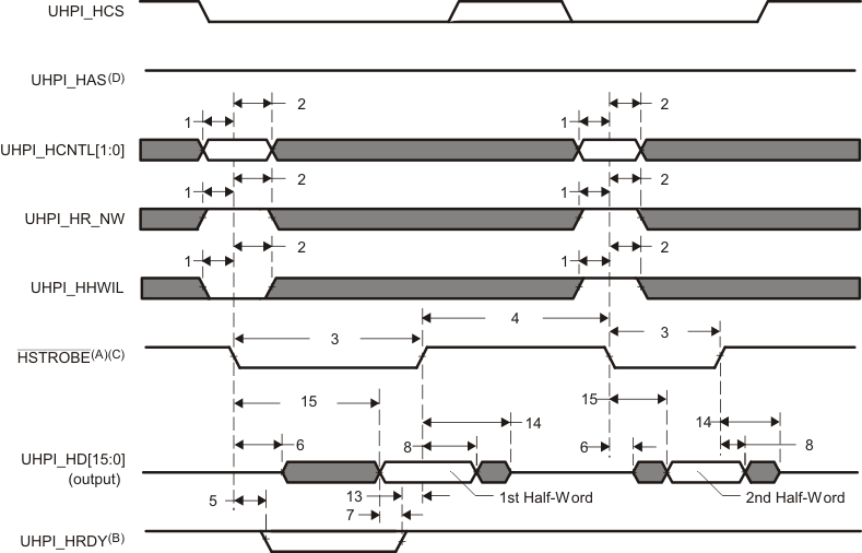
For more information on the UHPI peripheral, see the UHPI chapter in the TMS320C5517 Technical Reference Manual [literature number SPRUH16].
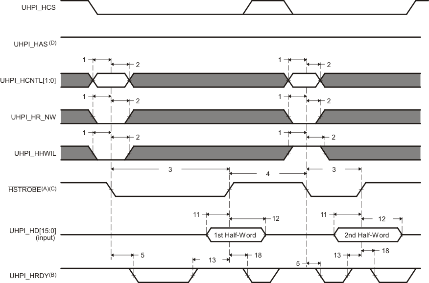
For more information on the UHPI peripheral, see the UHPI chapter in the TMs320C5517 Technical Reference Manual [literature number SPRUH16].
5.7.19 Universal Serial Bus (USB) 2.0 Controller
The device USB2.0 peripheral supports the following features:
- USB2.0 peripheral at speeds high-speed (480Mb/s) and full-speed (12Mb/s)
- All transfer modes (control, bulk, interrupt, and isochronous mode)
- 4 Transmit (TX) and 4 Receive (RX) Endpoints in addition to Control Endpoint 0
- FIFO RAM
- 4K endpoint
- Programmable size
- Integrated USB2.0 High Speed PHY
- RNDIS mode for accelerating RNDIS type protocols using short packet termination over USB
The USB2.0 peripheral on this device, does not support:
- Host Mode (Peripheral and Device Modes supported only)
- On-Chip Charge Pump
- On-the-Go (OTG) Mode
5.7.19.1 USB 2.0 Electrical Data and Timing
Table 5-64 Switching Characteristics Over Recommended Operating Conditions for USB 2.0 (see Figure 5-41)
| NO. | PARAMETER | CVDD = 1.05 V CVDD = 1.3 V CVDD = 1.4 V |
UNIT | ||||
|---|---|---|---|---|---|---|---|
| FULL SPEED 12 Mbps |
HIGH SPEED 480 Mbps(3) |
||||||
| MIN | MAX | MIN | MAX | ||||
| 1 | tr(D) | Rise time, USB_DP and USB_DM signals(4) | 4 | 20 | 0.5 | ns | |
| 2 | tf(D) | Fall time, USB_DP and USB_DM signals(4) | 4 | 20 | 0.5 | ns | |
| 3 | trfM | Rise and Fall time, matching(1) | 90 | 111 | – | – | % |
| 4 | VCRS | Output signal cross-over voltage(4) | 1.3 | 2 | – | – | V |
| 7 | tw(EOPT) | Pulse duration, EOP transmitter(2) | 160 | 175 | – | – | ns |
| 8 | tw(EOPR) | Pulse duration, EOP receiver(2) | 82 | – | ns | ||
| 9 | t(DRATE) | Data Rate | 12 | 480 | Mb/s | ||
| 10 | ZDRV | Driver Output Resistance | 40.5 | 49.5 | 40.5 | 49.5 | Ω |
| 11 | ZINP | Receiver Input Impedance | 100k | - | - | Ω | |
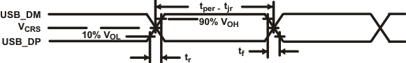 Figure 5-41 USB2.0 Integrated Transceiver Interface Timing
5.7.20 Emulation and Debug
5.7.20.1 Debugging Considerations
5.7.20.1.1 Pullup and Pulldown Resistors
Proper board design should ensure that input pins to the DSP are always at a valid logic level and not floating. This may be achieved via pullup and pulldown resistors. The DSP features internal pullup (IPU) and internal pulldown (IPD) resistors on many pins to eliminate the need, unless otherwise noted, for external pullup and pulldown resistors.
An external pullup and pulldown resistor may need to be used in the following situations:
- Configuration Pins: An external pullup and pulldown resistor is recommended to set the desired value or state (see the configuration pins listed in Table 5-5, Default Functions Affected by Device Configuration Pins). Note that some configuration pins must be connected directly to ground or to a specific supply voltage.
- Input Pins (I, I/O, I/O/Z): They are required to be driven at all times. To achieve the lowest power, input pins must not be allowed to float. When they are configured as input or tri-stated, and not driven to a known state, they may cause an excessive IO-supply current. Prevent this current by externally terminating it or enabling IPD and IPU, if applicable.
- Other Input Pins: If the IPU and IPD does not match the desired value or state, use an external pullup and pulldown resistor to pull the signal to the opposite rail.
For the configuration pins (listed in Table 5-5, Default Functions Affected by Device Configuration Pins), if they are both routed out and 3-stated (not driven), it is strongly recommended that an external pullup and pulldown resistor be implemented. In addition, applying external pullup and pulldown resistors on the configuration pins adds convenience to the user in debugging and flexibility in switching operating modes.
When an external pullup or pulldown resistor is used on a pin, the pin’s internal pullup or pulldown resistor should be disabled through the Pullup and Pulldown Inhibit Registers (PUDINHIBR1, 2, 3, 4, 5, 6, and 7) to minimize power consumption.
Tips for choosing an external pullup and pulldown resistor:
- Consider the total amount of current that may pass through the pullup or pulldown resistor. Make sure to include the leakage currents of all the devices connected to the net, as well as any internal pullup or pulldown (IPU and IPD) resistors.
- Decide a target value for the net. For a pulldown resistor, this should be below the lowest VIL level of all inputs connected to the net. For a pullup resistor, this should be above the highest VIH level of all inputs on the net. A reasonable choice would be to target the VOL or VOH levels for the logic family of the limiting device; which, by definition, have margin to the VIL and VIH levels.
- Select a pullup and pulldown resistor with the largest possible value; but, which can still ensure that the net will reach the target pulled value when maximum current from all devices on the net is flowing through the resistor. The current to be considered includes leakage current plus, any other internal and external pullup and pulldown resistors on the net.
- For bidirectional nets, there is an additional consideration which sets a lower limit on the resistance value of the external resistor. Verify that the resistance is small enough that the weakest output buffer can drive the net to the opposite logic level (including margin).
- Remember to include tolerances when selecting the resistor value.
- For pullup resistors, also remember to include tolerances on the DVDD rail.
For most systems, a 1-kΩ resistor can be used to oppose the IPU and IPD while meeting the above criteria. Users should confirm this resistor value is correct for their specific application.
For most systems, a 20-kΩ resistor can be used to compliment the IPU and IPD on the configuration pins while meeting the above criteria. Users should confirm this resistor value is correct for their specific application.
For more detailed information on input current (II), and the low- and high-level input voltages (VIL and VIH) for the device DSP, see Section 5.3.2, Electrical Characteristics.
For the internal pullup and pulldown resistors for all device pins, see the peripheral and system-specific signal descriptions table in this document.
5.7.20.1.2 Bus Holders
The device has special I/O bus-holder structures to ensure pins are not left floating when CVDD power is removed while I/O power is applied. When CVDD is "ON", the bus-holders are disabled and the internal pullups or pulldowns, if applicable, function normally. But when CVDD is "OFF" and the I/O supply is "ON", the bus-holders become enabled and any applicable internal pullups and pulldowns are disabled.
The bus-holders are weak drivers on the pin and, for as long as CVDD is "OFF" and I/O power is "ON", they hold the last state on the pin. If an external device is strongly driving the device I/O pin to the opposite state then the bus-holder will flip state to match the external driver and DC current will stop.
This bus-holder feature prevents unnecessary power consumption when CVDD is "OFF"and I/O supply is "ON". For example, current caused by undriven pins (input buffer oscillation) or DC current flowing through pullups or pulldowns.
If external pullup or pulldown resistors are implemented, then care should be taken that those pullup and pulldown resistors can exceed the internal bus-holder's max current and thereby cause the bus-holder to flip state to match the state of the external pullup or pulldown. Otherwise, DC current will flow unnecessarily. When CVDD power is applied, the bus holders are disabled (for further details on bus holders, see Section 5.7.2.3, Digital I/O Behavior When Core Power (CVDD) is Down).
5.7.20.1.3 CLKOUT Pin
For debug purposes, the DSP includes a CLKOUT pin which can be used to tap different clocks within the clock generator. The SRC bits of the CLKOUT Configuration Register (CLKOUTCR) can be used to specify the source for the CLKOUT pin.
Note: The bootloader disables the CLKOUT pin via CLKOFF bit in the ST3_55 CPU register.
For more information on the ST3_55 CPU register, see the C55x 3.0 CPU Reference Guide (literature number: SWPU073).
5.7.21 IEEE 1149.1 JTAG
The JTAG interface is used for Boundary-Scan testing and emulation of the device.
TRST should only to be deasserted when it is necessary to use a JTAG controller to debug the device or exercise the device's boundary scan functionality.
The device includes an internal pulldown (IPD) on the TRST pin to ensure that TRST will always be asserted upon power up and the device's internal emulation logic will always be properly initialized. An external pulldown should also be added to ensure proper device operation when an emulation or boundary scan JTAG controller is not connected to the JTAG pins. JTAG controllers from Texas Instruments actively drive TRST high. However, some third-party JTAG controllers may not drive TRST high but expect the use of a pullup resistor on TRST. When using this type of JTAG controller, assert TRST to initialize the device after powerup and externally drive TRST high before attempting any emulation or boundary scan operations. The device will not operate properly if TRST is not asserted low during powerup.
5.7.21.1 JTAG Test_port Electrical Data and Timing
Table 5-65 Timing Requirements for JTAG Test Port (see Figure 5-42)
| NO. | CVDD = 1.05 V CVDD = 1.3 V CVDD = 1.4 V |
UNIT | |||
|---|---|---|---|---|---|
| MIN | MAX | ||||
| 2 | tc(TCK) | Cycle time, TCK | 60 | ns | |
| 3 | tw(TCKH) | Pulse duration, TCK high | 24 | ns | |
| 4 | tw(TCKL) | Pulse duration, TCK low | 24 | ns | |
| 5 | tsu(TDIV-TCKH) | Setup time, TDI valid before TCK high | 10 | ns | |
| 6 | tsu(TMSV-TCKH) | Setup time, TMS valid before TCK high | 6 | ns | |
| 7 | th(TCKH-TDIV) | Hold time, TDI valid after TCK high | 5 | ns | |
| 8 | th(TCKH-TDIV) | Hold time, TMS valid after TCK high | 4 | ns | |
Table 5-66 Switching Characteristics Over Recommended Operating Conditions for JTAG Test Port
(see Figure 5-42)
| NO. | PARAMETER | CVDD = 1.05 V CVDD = 1.3 V CVDD = 1.4 V |
UNIT | ||
|---|---|---|---|---|---|
| MIN | MAX | ||||
| 1 | td(TCKL-TDOV) | Delay time, TCK low to TDO valid | 30.5 | ns | |
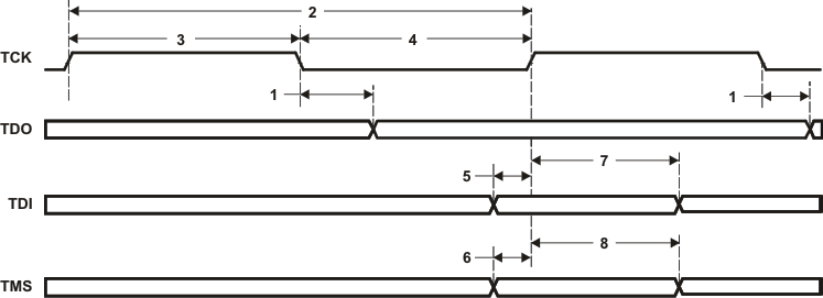 Figure 5-42 JTAG Test-Port Timing