SPRS727C August 2012 – April 2014 TMS320C5517
PRODUCTION DATA.
- 1Device Overview
- 2Revision History
- 3Device Comparison
-
4Terminal Configuration and Functions
- 4.1 Pin Diagram
- 4.2
Signal Descriptions
- 4.2.1 Oscillator and PLL
- 4.2.2 Real-Time Clock (RTC)
- 4.2.3 RESET, Interrupts, and JTAG
- 4.2.4 External Memory Interface (EMIF)
- 4.2.5 Inter-Integrated Circuit (I2C)
- 4.2.6 Inter-IC Sound (I2S)
- 4.2.7 Multichannel Buffered Serial Port (McBSP)
- 4.2.8 Multichannel Serial Port Interface (McSPI)
- 4.2.9 Serial Peripheral Interface (SPI)
- 4.2.10 Universal Asynchronous Receiver and Transmitter (UART)
- 4.2.11 Universal Serial Bus (USB) 2.0
- 4.2.12 Universal Host-Port Interface (UHPI)
- 4.2.13 MultiMedia Card (MMC)
- 4.2.14 Successive Approximation (SAR) Analog-to-Digital Converter (ADC)
- 4.2.15 General-Purpose Input and Output (GPIO)
- 4.2.16 Regulators and Power Management
- 4.2.17 Supply Voltage
- 4.2.18 Ground
- 4.3
Pin Multiplexing
- 4.3.1 UHPI, SPI, UART, I2S2, I2S3, and GP[31:27, 20:12] Pin Multiplexing [EBSR.PPMODE Bits]
- 4.3.2 MMC1, McSPI, and GP[11:6] Pin Multiplexing [EBSR.SP1MODE Bits]
- 4.3.3 MMC0, I2S0, McBSP, and GP[5:0] Pin Multiplexing [EBSR.SP0MODE Bits]
- 4.3.4 EMIF EM_A[20:15] and GP[26:21] Pin Multiplexing [EBSR.Axx_MODE bits]
- 4.4 Connections for Unused Signals
-
5Specifications
- 5.1 Absolute Maximum Ratings
- 5.2 Recommended Operating Conditions
- 5.3 Electrical Characteristics
- 5.4 Handling Ratings
- 5.5 Thermal Characteristics
- 5.6 Power-On Hours
- 5.7
Timing and Switching Characteristics
- 5.7.1 Parameter Information
- 5.7.2 Power Supplies
- 5.7.3
Reset
- 5.7.3.1 Power-On Reset (POR) Circuits
- 5.7.3.2 Pin Behavior at Reset
- 5.7.3.3 Reset Electrical Data and Timing
- 5.7.3.4 Configurations at Reset
- 5.7.3.5
Configurations After Reset
- 5.7.3.5.1 External Bus Selection Register (EBSR)
- 5.7.3.5.2 LDO Control Register [7004h]
- 5.7.3.5.3 EMIF and USB System Control Registers (ESCR and USBSCR) [1C33h and 1C32h]
- 5.7.3.5.4 Peripheral Clock Gating Control Registers (PCGCR1 and PCGCR2) [1C02h and 1C03h]
- 5.7.3.5.5 Pullup and Pulldown Inhibit Registers (PUDINHIBR1, 2, 3, 4, 5, 6, and 7) [1C17h, 1C18h, 1C19h, 1C4Ch, 1C4Dh, 1C4Fh, and 1C50h, respectively]
- 5.7.3.5.6 Output Slew Rate Control Register (OSRCR) [1C16h]
- 5.7.4
Clock Specifications
- 5.7.4.1 Recommended Clock and Control Signal Transition Behavior
- 5.7.4.2 Clock Considerations
- 5.7.4.3 PLLs
- 5.7.4.4 Input and Output Clocks Electrical Data and Timing
- 5.7.4.5 Wake-up Events, Interrupts, and XF
- 5.7.5 Direct Memory Access (DMA) Controller
- 5.7.6 External Memory Interface (EMIF)
- 5.7.7 General-Purpose Input/Output (GPIO)
- 5.7.8 Inter-Integrated Circuit (I2C)
- 5.7.9 Inter-IC Sound (I2S)
- 5.7.10 Multichannel Serial Port Interface (McSPI)
- 5.7.11 Multichannel Buffered Serial Port (McBSP)
- 5.7.12 Multimedia Card and Secure Digital (eMMC, MMC, SD, and SDHC)
- 5.7.13 Real-Time Clock (RTC)
- 5.7.14 SAR ADC (10-Bit)
- 5.7.15 Serial Port Interface (SPI)
- 5.7.16 Timers
- 5.7.17 Universal Asynchronous Receiver and Transmitter (UART)
- 5.7.18 Universal Host-Port Interface (UHPI)
- 5.7.19 Universal Serial Bus (USB) 2.0 Controller
- 5.7.20 Emulation and Debug
- 5.7.21 IEEE 1149.1 JTAG
-
6Detailed Description
- 6.1 CPU
- 6.2
Memory
- 6.2.1 Internal Memory
- 6.2.2 External Memory
- 6.2.3 Memory Map
- 6.2.4
Register Map
- 6.2.4.1 DMA Peripheral Register Description
- 6.2.4.2 EMIF Peripheral Register Description
- 6.2.4.3 GPIO Peripheral Register Description
- 6.2.4.4 I2C Peripheral Register Description
- 6.2.4.5 I2S Peripheral Register Description
- 6.2.4.6 McBSP Peripheral Register Descriptions
- 6.2.4.7 McSPI Peripheral Register Descriptions
- 6.2.4.8 MMC and SD Peripheral Register Description
- 6.2.4.9 RTC Peripheral Register Description
- 6.2.4.10 SAR ADC Peripheral Register Description
- 6.2.4.11 SPI Peripheral Register Descriptions
- 6.2.4.12 System Registers
- 6.2.4.13 Timers Peripheral Register Description
- 6.2.4.14 UART Peripheral Register Description
- 6.2.4.15 UHPI Peripheral Register Descriptions
- 6.2.4.16 USB2.0 Peripheral Register Descriptions
- 6.3 Identification
- 6.4 Boot Modes
- 7Device and Documentation Support
- 8Mechanical Packaging and Orderable Information
Package Options
Refer to the PDF data sheet for device specific package drawings
Mechanical Data (Package|Pins)
- ZCH|196
Thermal pad, mechanical data (Package|Pins)
Orderable Information
7 Device and Documentation Support
7.1 Device Support
7.1.1 Development Support
TI offers an extensive line of development tools for the TMS320C55x DSP platform, including tools to evaluate the performance of the processors, generate code, develop algorithm implementations, and fully integrate and debug software and hardware modules. The tool's support documentation is electronically available within the Code Composer Studio Integrated Development Environment (IDE).
The following products support development of TMS320C55x fixed-point DSP-based applications:
Software Development Tools:
Code Composer Studio Integrated Development Environment (IDE): Version 5.5.0 or later
C/C++/Assembly Code Generation, and Debug plus additional development tools
Scalable, Real-Time Foundation Software (DSP/BIOS Version 5.33 or later), which provides the basic run-time target software needed to support any DSP application.
Hardware Development Tools:
Extended Development System (XDS™) Emulator
For a complete listing of development-support tools for the TMS320C55x DSP platform, visit the Texas Instruments web site on the Worldwide Web at http://www.ti.com uniform resource locator (URL). For information on pricing and availability, contact the nearest TI field sales office or authorized distributor.
7.1.2 Device Nomenclature
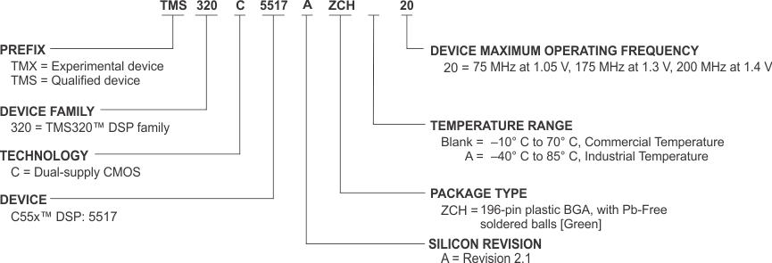
To designate the stages in the product development cycle, TI assigns prefixes to the part numbers of all DSP devices and support tools. Each DSP commercial family member has one of three prefixes: TMX, TMP, or TMS (for example, TMS320C5517AZCHA20). Texas Instruments recommends two of three possible prefix designators for its support tools: TMDX and TMDS. These prefixes represent evolutionary stages of product development from engineering prototypes (TMX or TMDX) through fully qualified production devices or tools (TMS or TMDS).
Device development evolutionary flow:
-
TMX Experimental device that is not necessarily representative of the final device's electrical specifications.
-
TMP Final silicon die that conforms to the device's electrical specifications but has not completed quality and reliability verification.
-
TMS Fully-qualified production device.
Support tool development evolutionary flow:
-
TMDX Development-support product that has not yet completed Texas Instruments internal qualification testing.
-
TMDS Fully qualified development-support product.
TMX and TMP devices and TMDX development-support tools are shipped against the following disclaimer:
"Developmental product is intended for internal evaluation purposes."
TMS devices and TMDS development-support tools have been characterized fully, and the quality and reliability of the device have been demonstrated fully. TI's standard warranty applies.
Predictions show that prototype devices (TMX or TMP) have a greater failure rate than the standard production devices. Texas Instruments recommends that these devices not be used in any production system because their expected end-use failure rate still is undefined. Only qualified production devices are to be used.
TI device nomenclature also includes a suffix with the device family name. This suffix indicates the package type (for example, ZCH), and the temperature range (for example, "Blank" is the commercial temperature range).
Figure 7-1 provides a legend for reading the complete device name for any DSP platform member.
7.2 Documentation Support
7.2.1 Related Documentation
The following documents describe the DSP. To access the documents, click the literature number (e.g., SPRUH16) or wiki link.
The current documentation that describes the DSP, related peripherals, and other technical collateral, is available in the product folder at www.ti.com.
-
SPRUH16TMS320C5517 Digital Signal Processor Technical Reference Manual. Collection of documents providing detailed information on the device including system control, FFT implementation, and memory access. Detailed information on the device as well as a functional description of the peripherals supported is also included.
-
SPRZ383TMS320C5517 Fixed-Point Digital Signal Processor Silicon Errata. Describes the known exceptions to the functional specifications for this device.
-
SPRABP1Using the TMS320C5517 Bootloader. Describes features of the on-chip ROM for this device, as well as descriptions of how to interface with possible boot devices and generating a boot image to store on an external device.
-
SWPU073 TMS320C55x DSP v3.x CPU Reference Guide. Describes more detailed information on the C55x CPU.
-
WikiC5505/15/35 Schematic Checklist. Describes recommendations for the device applicable to unused pins, clocking, power, reset, and peripherals. Description also includes critical connections, DDR2 routing checklist, and debug considerations, and more.
7.3 Community Resources
The following links connect to TI community resources. Linked contents are provided "AS IS" by the respective contributors. They do not constitute TI specifications and do not necessarily reflect TI's views; see TI's Terms of Use.
-
TI E2E™ Online Community TI's Engineer-to-Engineer (E2E) Community. Created to foster collaboration among engineers. At e2e.ti.com, you can ask questions, share knowledge, explore ideas and help solve problems with fellow engineers.
-
TI Embedded Processors Wiki Texas Instruments Embedded Processors Wiki. Established to help developers get started with Embedded Processors from Texas Instruments and to foster innovation and growth of general knowledge about the hardware and software surrounding these devices.
7.4 Trademarks
C5000, eXpressDSP, Code Composer Studio, DSP/BIOS, RTDX, XDS510, XDS560, XDS, E2E are trademarks of Texas Instruments.
All other trademarks are the property of their respective owners.
7.5 Electrostatic Discharge Caution

This integrated circuit can be damaged by ESD. Texas Instruments recommends that all integrated circuits be handled with appropriate precautions. Failure to observe proper handling and installation procedures can cause damage.
ESD damage can range from subtle performance degradation to complete device failure. Precision integrated circuits may be more susceptible to damage because very small parametric changes could cause the device not to meet its published specifications.
7.6 Glossary
SLYZ022 — TI Glossary.
This glossary lists and explains terms, acronyms and definitions.