SPRSP19 December 2017 TMS320F28377D-EP
PRODUCTION DATA.
- 1Device Overview
- 2Revision History
- 3Terminal Configuration and Functions
-
4Specifications
- 4.1 Absolute Maximum Ratings
- 4.2 ESD Ratings
- 4.3 Recommended Operating Conditions
- 4.4 Power Consumption Summary
- 4.5 Electrical Characteristics
- 4.6 Thermal Resistance Characteristics
- 4.7
System
- 4.7.1 Power Sequencing
- 4.7.2 Reset Timing
- 4.7.3 Clock Specifications
- 4.7.4 Flash Parameters
- 4.7.5 Emulation/JTAG
- 4.7.6 GPIO Electrical Data and Timing
- 4.7.7 Interrupts
- 4.7.8 Low-Power Modes
- 4.7.9 External Memory Interface (EMIF)
- 4.8 Analog Peripherals
- 4.9 Control Peripherals
- 4.10
Communications Peripherals
- 4.10.1 Controller Area Network (CAN)
- 4.10.2 Inter-Integrated Circuit (I2C)
- 4.10.3 Multichannel Buffered Serial Port (McBSP)
- 4.10.4 Serial Communications Interface (SCI)
- 4.10.5 Serial Peripheral Interface (SPI)
- 4.10.6 Universal Serial Bus (USB) Controller
- 4.10.7 Universal Parallel Port (uPP) Interface
-
5Detailed Description
- 5.1 Overview
- 5.2 Functional Block Diagram
- 5.3 Memory
- 5.4 Identification
- 5.5 Bus Architecture - Peripheral Connectivity
- 5.6 C28x Processor
- 5.7 Control Law Accelerator
- 5.8 Direct Memory Access
- 5.9 Interprocessor Communication Module
- 5.10 Boot ROM and Peripheral Booting
- 5.11 Dual Code Security Module
- 5.12 Timers
- 5.13 Nonmaskable Interrupt With Watchdog Timer (NMIWD)
- 5.14 Watchdog
- 5.15 Configurable Logic Block (CLB)
- 6Applications, Implementation, and Layout
- 7Device and Documentation Support
- 8Mechanical, Packaging, and Orderable Information
Package Options
Mechanical Data (Package|Pins)
Thermal pad, mechanical data (Package|Pins)
- PTP|176
Orderable Information
4 Specifications
4.1 Absolute Maximum Ratings(1)(2)
over operating free-air temperature range (unless otherwise noted)| MIN | MAX | UNIT | ||
|---|---|---|---|---|
| Supply voltage | VDDIO with respect to VSS | –0.3 | 4.6 | V |
| VDD3VFL with respect to VSS | –0.3 | 4.6 | ||
| VDDOSC with respect to VSS | –0.3 | 4.6 | ||
| VDD with respect to VSS | –0.3 | 1.5 | ||
| Analog voltage | VDDA with respect to VSSA | –0.3 | 4.6 | V |
| Input voltage | VIN (3.3 V) | –0.3 | 4.6 | V |
| Output voltage | VO | –0.3 | 4.6 | V |
| Input clamp current | Digital input (per pin), IIK (VIN < VSS or VIN > VDDIO) | –20 | 20 | mA |
| Analog input (per pin), IIKANALOG
(VIN < VSSA or VIN > VDDA) |
–20 | 20 | ||
| Total for all inputs, IIKTOTAL
(VIN < VSS/VSSA or VIN > VDDIO/VDDA) |
–20 | 20 | ||
| Output current | Digital output (per pin), IOUT | –20 | 20 | mA |
| Operating junction temperature | TJ | –55 | 150 | °C |
| Storage temperature(3) | Tstg | –65 | 150 | °C |
4.2 ESD Ratings
| VALUE | UNIT | ||||
|---|---|---|---|---|---|
| TMS320F28377D in 337-ball ZWT package | |||||
| V(ESD) | Electrostatic discharge (ESD) | Human-body model (HBM), per ANSI/ESDA/JEDEC JS-001(1) | ±2000 | V | |
| Charged-device model (CDM), per JEDEC specification JESD22-C101(2) | ±500 | ||||
| TMS320F28377D in 176-pin PTP package | |||||
| V(ESD) | Electrostatic discharge (ESD) | Human-body model (HBM), per ANSI/ESDA/JEDEC JS-001(1) | ±2000 | V | |
| Charged-device model (CDM), per JEDEC specification JESD22-C101(2) | ±500 | ||||
4.3 Recommended Operating Conditions
| MIN | NOM | MAX | UNIT | ||
|---|---|---|---|---|---|
| Device supply voltage, I/O, VDDIO(1) | 3.14 | 3.3 | 3.47 | V | |
| Device supply voltage, VDD | 1.14 | 1.2 | 1.26 | V | |
| Supply ground, VSS | 0 | V | |||
| Analog supply voltage, VDDA | 3.14 | 3.3 | 3.47 | V | |
| Analog ground, VSSA | 0 | V | |||
| Junction temperature, TJ (2) | –55 | 125 | °C | ||
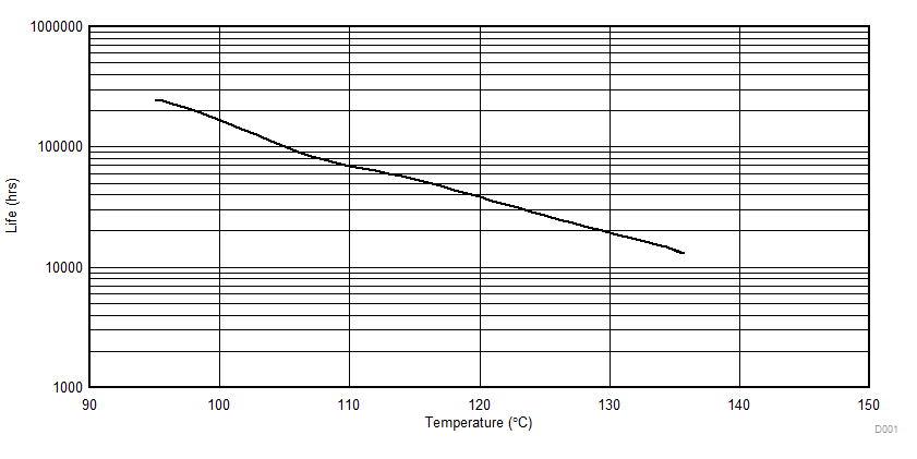
4.4 Power Consumption Summary
Current values listed in this section are representative for the test conditions given and not the absolute maximum possible. The actual device currents in an application will vary with application code and pin configurations. Table 4-1 shows the device current consumption at 200-MHz SYSCLK.
Table 4-1 Device Current Consumption at 200-MHz SYSCLK
| MODE | TEST CONDITIONS | IDD | IDDIO(1) | IDDA | IDD3VFL | ||||
|---|---|---|---|---|---|---|---|---|---|
| TYP(5) | MAX(4) | TYP(5) | MAX(4) | TYP(5) | MAX(4) | TYP(5) | MAX(4) | ||
| Operational (RAM) |
|
325 mA | 440 mA | 30 mA | 13 mA | 20 mA | 33 mA | 40 mA | |
| IDLE |
|
105 mA | 210 mA | 3 mA | 10 mA | 10 µA | 150 µA | 10 µA | 150 µA |
| STANDBY |
|
30 mA | 135 mA | 3 mA | 10 mA | 5 µA | 150 µA | 10 µA | 150 µA |
| HALT(2) |
|
1.5 mA | 110 mA | 750 µA | 2 mA | 5 µA | 150 µA | 10 µA | 150 µA |
| HIBERNATE(3) |
|
300 µA | 4 mA | 750 µA | 2 mA | 5 µA | 75 µA | 1 µA | 50 µA |
| Flash Erase/Program |
|
242 mA | 360 mA | 3 mA | 10 mA | 10 µA | 150 µA | 53 mA | 65 mA |
- All of the communication peripherals are exercised in loop-back mode: CAN-A to CAN-B; SPI-A to SPI-C; SCI-A to SCI-D; I2C-A to I2C-B; McBSP-A to McBSP-B; USB
- SDFM1 to SDFM4 active
- ePWM1 to ePWM12 generate 400-kHz PWM output on 24 pins
- CPU TIMERs active
- DMA does 32-bit burst transfers
- CLA1 does multiply-accumulate tasks
- All ADCs perform continuous conversion
- All DACs ramp voltage up/down at 150 kHz
- CMPSS1 to CMPSS8 active
The following is executed in a loop on CPU2:
- CPU TIMERs active
- CLA1 does multiply-accumulate tasks
- VCU does complex multiply/accumulate with parallel load
- TMU calculates a cosine
- FPU does multiply/accumulate with parallel load
4.4.1 Current Consumption Graphs
Figure 4-2 and Figure 4-3 are a typical representation of the relationship between frequency and current consumption/power on the device. The operational test from Table 4-1 was run across frequency at Vmax and high temperature. Actual results will vary based on the system implementation and conditions.
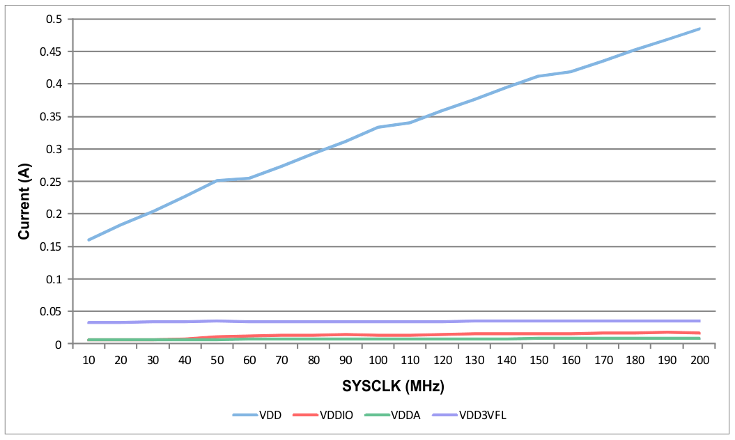 Figure 4-2 Operational Current Versus Frequency
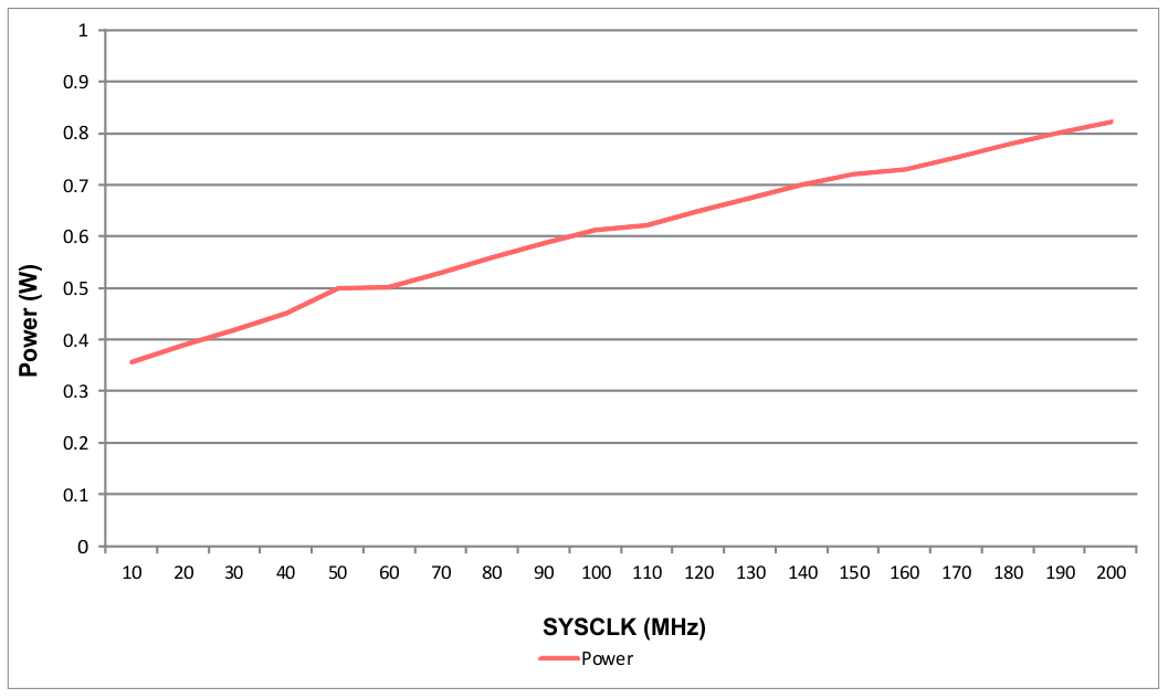 Figure 4-3 Power Versus Frequency
Leakage current will increase with operating temperature in a nonlinear manner. The difference in VDD current between TYP and MAX conditions can be seen in Figure 4-4. The current consumption in HALT mode is primarily leakage current as there is no active switching if the internal oscillator has been powered down.
Figure 4-4 shows the typical leakage current across temperature. The device was placed into HALT mode under nominal voltage conditions.
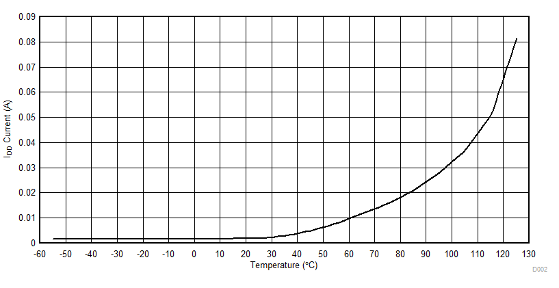 Figure 4-4 IDD Leakage Current Versus Temperature
4.4.2 Reducing Current Consumption
The F28377D provides some methods to reduce the device current consumption:
- Any one of the four low-power modes—IDLE, STANDBY, HALT, and HIBERNATE—could be entered during idle periods in the application.
- The flash module may be powered down if the code is run from RAM.
- Disable the pullups on pins that assume an output function.
- Each peripheral has an individual clock-enable bit (PCLKCRx). Reduced current consumption may be achieved by turning off the clock to any peripheral that is not used in a given application. Table 4-2 indicates the typical current reduction that may be achieved by disabling the clocks using the PCLKCRx register.
Table 4-2 Current on VDD Supply by Various Peripherals (at 200 MHz)(1)
| PERIPHERAL MODULE(2) |
IDD CURRENT REDUCTION (mA) |
|---|---|
| ADC(3) | 3.3 |
| CAN | 3.3 |
| CLA | 1.4 |
| CMPSS(3) | 1.4 |
| CPUTIMER | 0.3 |
| DAC(3) | 0.6 |
| DMA | 2.9 |
| eCAP | 0.6 |
| EMIF1 | 2.9 |
| EMIF2 | 2.6 |
| ePWM1 to ePWM4(4) | 4.5 |
| ePWM5 to ePWM12(4) | 1.7 |
| HRPWM(4) | 1.7 |
| I2C | 1.3 |
| McBSP | 1.6 |
| SCI | 0.9 |
| SDFM | 2 |
| SPI | 0.5 |
| uPP | 7.3 |
| USB and AUXPLL at 60 MHz | 23.8 |
4.5 Electrical Characteristics
over recommended operating conditions (unless otherwise noted)| PARAMETER | TEST CONDITIONS | MIN | TYP | MAX | UNIT | ||
|---|---|---|---|---|---|---|---|
| VOH | High-level output voltage | IOH = IOH MIN | VDDIO * 0.8 | V | |||
| IOH = –100 μA | VDDIO – 0.2 | ||||||
| VOL | Low-level output voltage | IOL = IOL MAX | 0.4 | V | |||
| IOL = 100 µA | 0.2 | ||||||
| IOH | High-level output source current for all output pins | –4 | mA | ||||
| IOL | Low-level output sink current for all output pins | 4 | mA | ||||
| VIH | High-level input voltage (3.3 V) | GPIO0–GPIO7, GPIO42–GPIO43, GPIO46–GPIO47 |
VDDIO * 0.7 | VDDIO + 0.3 | V | ||
| All other pins | 2.0 | VDDIO + 0.3 | |||||
| VIL | Low-level input voltage (3.3 V) | VSS – 0.3 | 0.8 | V | |||
| Ipulldown | Input current | Digital inputs with pulldown(1) | VDDIO = 3.3 V VIN = VDDIO |
120 | µA | ||
| Ipullup | Input current | Digital inputs with pullup enabled(1) | VDDIO = 3.3 V VIN = 0 V |
150 | µA | ||
| ILEAK | Pin leakage | Digital | Pullups disabled 0 V ≤ VIN ≤ VDDIO |
2 | µA | ||
| Analog (except ADCINB0 or DACOUTx) | 0 V ≤ VIN ≤ VDDA | 2 | |||||
| ADCINB0 | 2 | 11(2) | |||||
| DACOUTx | 66 | ||||||
| CI | Input capacitance | 2 | pF | ||||
4.6 Thermal Resistance Characteristics
4.6.1 GWT Package
| °C/W(1) | AIR FLOW (lfm)(2) | ||
|---|---|---|---|
| RΘJC | Junction-to-case thermal resistance | 8.8 | N/A |
| RΘJB | Junction-to-board thermal resistance | 11.6 | N/A |
| RΘJA (High k PCB) | Junction-to-free air thermal resistance | 23.2 | 0 |
| RΘJMA | Junction-to-moving air thermal resistance | 19.0 | 150 |
| 17.8 | 250 | ||
| 16.5 | 500 | ||
| PsiJT | Junction-to-package top | 0.2 | 0 |
| 0.3 | 150 | ||
| 0.4 | 250 | ||
| 0.5 | 500 | ||
| PsiJB | Junction-to-board | 11.4 | 0 |
| 11.3 | 150 | ||
| 11.2 | 250 | ||
| 11.0 | 500 |
- JESD51-2, Integrated Circuits Thermal Test Method Environmental Conditions - Natural Convection (Still Air)
- JESD51-3, Low Effective Thermal Conductivity Test Board for Leaded Surface Mount Packages
- JESD51-7, High Effective Thermal Conductivity Test Board for Leaded Surface Mount Packages
- JESD51-9, Test Boards for Area Array Surface Mount Package Thermal Measurements
4.6.2 PTP Package
| °C/W(1) | AIR FLOW (lfm)(2) | ||
|---|---|---|---|
| RΘJC | Junction-to-case thermal resistance | 10.2 | N/A |
| RΘJB | Junction-to-board thermal resistance | 7.9 | N/A |
| RΘJA (High k PCB) | Junction-to-free air thermal resistance | 19.4 | 0 |
| RΘJMA | Junction-to-moving air thermal resistance | 12.8 | 150 |
| 11.4 | 250 | ||
| 10.1 | 500 | ||
| PsiJT | Junction-to-package top | 0.11 | 0 |
| 0.24 | 150 | ||
| 0.33 | 250 | ||
| 0.42 | 500 | ||
| PsiJB | Junction-to-board | 6.1 | 0 |
| 5.5 | 150 | ||
| 5.4 | 250 | ||
| 5.3 | 500 |
- JESD51-2, Integrated Circuits Thermal Test Method Environmental Conditions - Natural Convection (Still Air)
- JESD51-3, Low Effective Thermal Conductivity Test Board for Leaded Surface Mount Packages
- JESD51-7, High Effective Thermal Conductivity Test Board for Leaded Surface Mount Packages
- JESD51-9, Test Boards for Area Array Surface Mount Package Thermal Measurements
4.7 System
4.7.1 Power Sequencing
An external power supply must be used to supply 3.3 V to VDDIO, VDD3VFL, VDDOSC, and VDDA and to provide 1.2 V to VDD. The internal VREG is not supported; therefore, the VREGENZ pin must be tied high to 3.3 V. The supplies should ramp to full rail within 10 ms. Table 4-3 shows the supply ramp rate.
Table 4-3 Supply Ramp Rate
| MIN | MAX | UNIT | ||
|---|---|---|---|---|
| Supply ramp rate | VDDIO, VDD, VDDA, VDD3VFL, VDDOSC with respect to VSS | 330 | 105 | V/s |
The voltage on VDDIO should be greater than VDD or no less than 0.3 V below VDD at all times. VDDIO, VDD3VFL, VDDOSC, and VDDA should be powered up together and be kept within 0.3 V of each other during operation. Before powering the device, no voltage larger than 0.3 V above VDDIO should be applied to any digital pin, and no voltage larger than 0.3 V above VDDA should be applied to any analog pin. The VREFHI voltage should not exceed VDDA at any time.
An internal power-on-reset (POR) circuit holds the device in reset and keeps the I/Os in a high-impedance state during power up. External supply voltage supervisors (SVS) can be used to monitor the voltage on the 3.3-V and 1.2-V rails and drive XRS low should supplies fall outside operational specifications.
4.7.2 Reset Timing
XRS is the device reset pin. It functions as an input and open-drain output. The device has a built-in power-on reset (POR). During power up, the POR circuit drives the XRS pin low. A watchdog or NMI watchdog reset also drives the pin low. An external circuit may drive the pin to assert a device reset.
A resistor with a value from 2.2 kΩ to 10 kΩ should be placed between XRS and VDDIO. A capacitor should be placed between XRS and VSS for noise filtering; the capacitance should be 100 nF or smaller. These values will allow the watchdog to properly drive the XRS pin to VOL within 512 OSCCLK cycles when the watchdog reset is asserted. Figure 4-5 shows the recommended reset circuit.
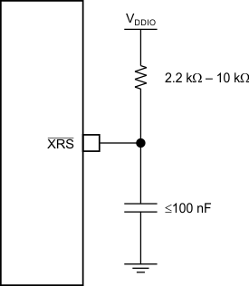 Figure 4-5 Reset Circuit
4.7.2.1 Reset Sources
The following reset sources exist on this device: XRS, WDRS, NMIWDRS, SYSRS, SCCRESET, and HIBRESET. See the Reset Signals table in the System Control chapter of the TMS320F2837xD Dual-Core Delfino Microcontrollers Technical Reference Manual.
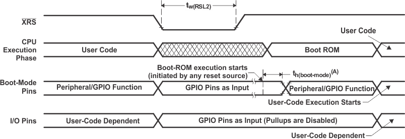
The parameter th(boot-mode) must account for a reset initiated from any of these sources.
CAUTION
Some reset sources are internally driven by the device. Some of these sources will drive XRS low. Use this to disable any other devices driving the boot pins. The SCCRESET and debugger reset sources do not drive XRS; therefore, the pins used for boot mode should not be actively driven by other devices in the system. The boot configuration has a provision for changing the boot pins in OTP; for more details, see the TMS320F2837xD Dual-Core Delfino Microcontrollers Technical Reference Manual.
4.7.2.2 Reset Electrical Data and Timing
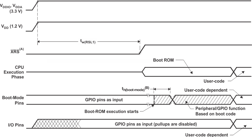
Table 4-4 shows the reset (XRS) timing requirements. Table 4-5 shows the reset (XRS) switching characteristics. Figure 4-6 shows the power-on reset. Figure 4-7 shows the warm reset.
Table 4-4 Reset (XRS) Timing Requirements
| MIN | MAX | UNIT | ||
|---|---|---|---|---|
| th(boot-mode) | Hold time for boot-mode pins | 1.5 | ms | |
| tw(RSL2) | Pulse duration, XRS low on warm reset | 3.2 | µs | |
Table 4-5 Reset (XRS) Switching Characteristics
over recommended operating conditions (unless otherwise noted)| PARAMETER | MIN | TYP | MAX | UNIT | |
|---|---|---|---|---|---|
| tw(RSL1) | Pulse duration, XRS driven low by device after supplies are stable | 100 | µs | ||
| tw(WDRS) | Pulse duration, reset pulse generated by watchdog | 512tc(OSCCLK) | cycles | ||
4.7.3 Clock Specifications
4.7.3.1 Clock Sources
Table 4-6 lists four possible clock sources. Figure 4-8 provides an overview of the device's clocking system.
Table 4-6 Possible Reference Clock Sources
| CLOCK SOURCE | MODULES CLOCKED | COMMENTS |
|---|---|---|
| INTOSC1 | Can be used to provide clock for:
|
Internal oscillator 1. Zero-pin overhead 10-MHz internal oscillator. |
| INTOSC2(1) | Can be used to provide clock for:
|
Internal oscillator 2. Zero-pin overhead 10-MHz internal oscillator. |
| XTAL | Can be used to provide clock for:
|
External crystal or resonator connected between the X1 and X2 pins or single-ended clock connected to the X1 pin. |
| AUXCLKIN | Can be used to provide clock for:
|
Single-ended 3.3-V level clock source. GPIO133/AUXCLKIN pin should be used to provide the input clock. |
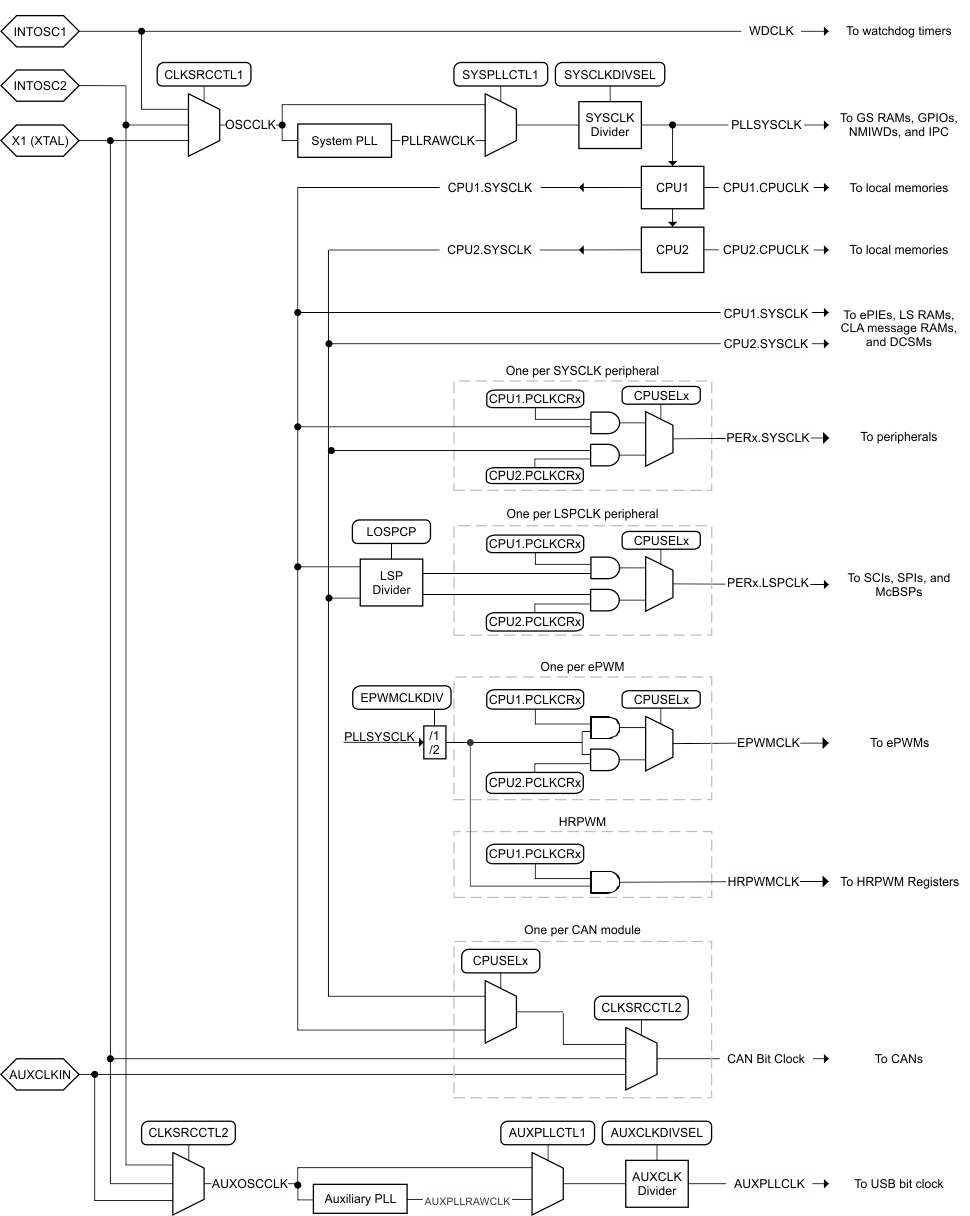 Figure 4-8 Clocking System
4.7.3.2 Clock Frequencies, Requirements, and Characteristics
This section provides the frequencies and timing requirements of the input clocks, PLL lock times, frequencies of the internal clocks, and the frequency and switching characteristics of the output clock.
4.7.3.2.1 Input Clock Frequency and Timing Requirements, PLL Lock Times
Table 4-7 shows the frequency requirements for the input clocks. Table 4-16 shows the crystal equivalent series resistance requirements. Table 4-8 shows the X1 input level characteristics when using an external clock source. Table 4-9 and Table 4-10 show the timing requirements for the input clocks. Table 4-11 shows the PLL lock times for the Main PLL and the USB PLL.
Table 4-7 Input Clock Frequency
| MIN | MAX | UNIT | |||
|---|---|---|---|---|---|
| f(XTAL) | Frequency, X1/X2, from external crystal or resonator | 10 | 20 | MHz | |
| f(X1) | Frequency, X1, from external oscillator (PLL enabled) | 2 | 25 | MHz | |
| Frequency, X1, from external oscillator (PLL disabled) | 2 | 100 | MHz | ||
| f(AUXI) | Frequency, AUXCLKIN, from external oscillator | 2 | 60 | MHz | |
Table 4-8 X1 Input Level Characteristics When Using an External Clock Source (Not a Crystal)
over recommended operating conditions (unless otherwise noted)| PARAMETER | MIN | MAX | UNIT | |
|---|---|---|---|---|
| X1 VIL | Valid low-level input voltage | –0.3 | 0.3 * VDDIO | V |
| X1 VIH | Valid high-level input voltage | 0.7 * VDDIO | VDDIO + 0.3 | V |
Table 4-9 X1 Timing Requirements
| MIN | MAX | UNIT | |||
|---|---|---|---|---|---|
| tf(X1) | Fall time, X1 | 6 | ns | ||
| tr(X1) | Rise time, X1 | 6 | ns | ||
| tw(X1L) | Pulse duration, X1 low as a percentage of tc(X1) | 45% | 55% | ||
| tw(X1H) | Pulse duration, X1 high as a percentage of tc(X1) | 45% | 55% | ||
Table 4-10 AUXCLKIN Timing Requirements
| MIN | MAX | UNIT | |||
|---|---|---|---|---|---|
| tf(AUXI) | Fall time, AUXCLKIN | 6 | ns | ||
| tr(AUXI) | Rise time, AUXCLKIN | 6 | ns | ||
| tw(AUXL) | Pulse duration, AUXCLKIN low as a percentage of tc(XCI) | 45% | 55% | ||
| tw(AUXH) | Pulse duration, AUXCLKIN high as a percentage of tc(XCI) | 45% | 55% | ||
Table 4-11 PLL Lock Times
| MIN | NOM | MAX | UNIT | ||
|---|---|---|---|---|---|
| t(PLL) | Lock time, Main PLL (X1, from external oscillator) | 50 µs + 2500 * tc(OSCCLK)(1) | µs | ||
| t(USB) | Lock time, USB PLL (AUXCLKIN, from external oscillator) | 50 µs + 2500 * tc(OSCCLK)(1) | µs | ||
4.7.3.2.2 Internal Clock Frequencies
Table 4-12 provides the clock frequencies for the internal clocks.
Table 4-12 Internal Clock Frequencies
| MIN | NOM | MAX | UNIT | ||
|---|---|---|---|---|---|
| f(SYSCLK) | Frequency, device (system) clock | 2 | 200(3) | MHz | |
| tc(SYSCLK) | Period, device (system) clock | 5(3) | 500 | ns | |
| f(PLLRAWCLK) | Frequency, system PLL output (before SYSCLK divider) | 120 | 400 | MHz | |
| f(AUXPLLRAWCLK) | Frequency, auxiliary PLL output (before AUXCLK divider) | 120 | 400 | MHz | |
| f(AUXPLL) | Frequency, AUXPLLCLK | 2 | 60 | 60 | MHz |
| f(PLL) | Frequency, PLLSYSCLK | 2 | 200(3) | MHz | |
| f(LSP) | Frequency, LSPCLK(1) | 2 | 200(3) | MHz | |
| tc(LSPCLK) | Period, LSPCLK | 5(3) | 500 | ns | |
| f(OSCCLK) | Frequency, OSCCLK (INTOSC1 or INTOSC2 or XTAL or X1) | See respective clock | MHz | ||
| f(EPWM) | Frequency, EPWMCLK(2) | 100 | MHz | ||
| f(HRPWM) | Frequency, HRPWMCLK | 60 | 100 | MHz | |
4.7.3.2.3 Output Clock Frequency and Switching Characteristics
Table 4-13 provides the frequency of the output clock. Table 4-14 shows the switching characteristics of the output clock, XCLKOUT.
Table 4-13 Output Clock Frequency
| MIN | MAX | UNIT | |||
|---|---|---|---|---|---|
| f(XCO) | Frequency, XCLKOUT | 50 | MHz | ||
Table 4-14 XCLKOUT Switching Characteristics (PLL Bypassed or Enabled)(1)(2)
over recommended operating conditions (unless otherwise noted)| PARAMETER | MIN | MAX | UNIT | ||
|---|---|---|---|---|---|
| tf(XCO) | Fall time, XCLKOUT | 5 | ns | ||
| tr(XCO) | Rise time, XCLKOUT | 5 | ns | ||
| tw(XCOL) | Pulse duration, XCLKOUT low | H – 2 | H + 2 | ns | |
| tw(XCOH) | Pulse duration, XCLKOUT high | H – 2 | H + 2 | ns | |
4.7.3.3 Input Clocks and PLLs
In addition to the internal 0-pin oscillators, multiple external clock source options are available. Figure 4-9 shows the recommended methods of connecting crystals, resonators, and oscillators to pins X1/X2 (also referred to as XTAL) and AUXCLKIN.
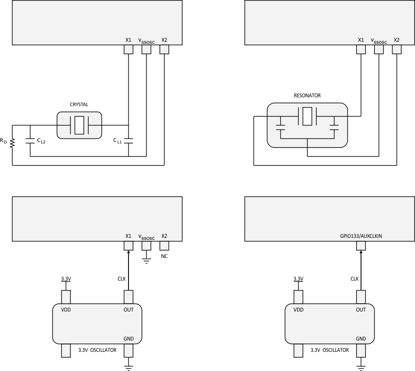 Figure 4-9 Connecting Input Clocks to a 2837xD Device
4.7.3.4 Crystal Oscillator
When using a quartz crystal, it may be necessary to include a damping resistor (RD) in the crystal circuit to prevent over-driving the crystal (drive level can be found in the crystal data sheet). In higher-frequency applications (10 MHz or greater), RD is generally not required. If a damping resistor is required, RD should be as small as possible because the size of the resistance affects start-up time (smaller RD = faster start-up time). TI recommends that the crystal manufacturer characterize the crystal with the application board. Table 4-15 shows the crystal oscillator parameters. Table 4-16 shows the crystal equivalent series resistance (ESR) requirements. Table 4-17 shows the crystal oscillator electrical characteristics.
Table 4-15 Crystal Oscillator Parameters
| MIN | MAX | UNIT | |||
|---|---|---|---|---|---|
| CL1, CL2 | Load capacitance | 12 | 24 | pF | |
| C0 | Crystal shunt capacitance | 7 | pF | ||
Table 4-16 Crystal Equivalent Series Resistance (ESR) Requirements(1)(2)
| CRYSTAL FREQUENCY (MHz) | MAXIMUM ESR (Ω) (CL1 = CL2 = 12 pF) |
MAXIMUM ESR (Ω) (CL1 = CL2 = 24 pF) |
|---|---|---|
| 10 | 55 | 110 |
| 12 | 50 | 95 |
| 14 | 50 | 90 |
| 16 | 45 | 75 |
| 18 | 45 | 65 |
| 20 | 45 | 50 |
Table 4-17 Crystal Oscillator Electrical Characteristics
over recommended operating conditions (unless otherwise noted)| PARAMETER | TEST CONDITIONS | MIN | TYP | MAX | UNIT | |
|---|---|---|---|---|---|---|
| Start-up time(1) | f = 20 MHz ESR MAX = 50 Ω CL1 = CL2 = 24 pF C0 = 7 pF |
2 | ms | |||
| Crystal drive level (DL) | 1 | mW | ||||
4.7.3.5 Internal Oscillators
To reduce production board costs and application development time, the F28377D contains two independent internal oscillators, referred to as INTOSC1 and INTOSC2. By default, both oscillators are enabled at power up. INTOSC2 is set as the source for the system reference clock (OSCCLK) and INTOSC1 is set as the backup clock source. INTOSC1 can also be manually configured as the system reference clock (OSCCLK). Table 4-18 provides the electrical characteristics of the internal oscillators to determine if this module meets the clocking requirements of the application.
Table 4-18 provides the electrical characteristics of the two internal oscillators.
NOTE
This oscillator cannot be used as the PLL source if the PLLSYSCLK is configured to frequencies above 194 MHz.
Table 4-18 Internal Oscillator Electrical Characteristics
over recommended operating conditions (unless otherwise noted)| PARAMETER | TEST CONDITIONS | MIN | TYP | MAX | UNIT | |
|---|---|---|---|---|---|---|
| f(INTOSC) | Frequency, INTOSC1 and INTOSC2 | 9.7 | 10.0 | 10.3 | MHz | |
| f(INTOSC-STABILITY) | Frequency stability at room temperature | 30ºC, Nominal VDD | ±0.1% | |||
| Frequency stability over VDD | 30ºC | ±0.2% | ||||
| Frequency stability | –3.0% | 3.0% | ||||
| f(INTOSC-ST) | Start-up and settling time | 20 | µs | |||
4.7.4 Flash Parameters
The on-chip flash memory is tightly integrated to the CPU, allowing code execution directly from flash through 128-bit-wide prefetch reads and a pipeline buffer. Flash performance for sequential code is equal to execution from RAM. Factoring in discontinuities, most applications will run with an efficiency of approximately 80% relative to code executing from RAM. This flash efficiency lets designers realize a 2× improvement in performance when migrating from the previous generation Delfino MCUs.
This device also has an OTP (One-Time-Programmable) sector used for the dual code security module (DCSM), which cannot be erased after it is programmed.
Table 4-19 shows the minimum required flash wait states at different frequencies. Table 4-20 shows the flash parameters.
Table 4-19 Flash Wait States
| CPUCLK (MHz) | MINIMUM WAIT STATES (1) | |
|---|---|---|
| EXTERNAL OSCILLATOR OR CRYSTAL | INTOSC1 OR INTOSC2 | |
| 150 < CPUCLK ≤ 200 | 145 < CPUCLK ≤ 194 | 3 |
| 100 < CPUCLK ≤ 150 | 97 < CPUCLK ≤ 145 | 2 |
| 50 < CPUCLK ≤ 100 | 48 < CPUCLK ≤ 97 | 1 |
| CPUCLK ≤ 50 | CPUCLK ≤ 48 | 0 |
Table 4-20 Flash Parameters
| PARAMETER | MIN | TYP | MAX | UNIT | ||
|---|---|---|---|---|---|---|
| Program Time(1) | 128 data bits + 16 ECC bits | 40 | 300 | µs | ||
| 8KW sector | 90 | 180 | ms | |||
| 32KW sector | 360 | 720 | ms | |||
| Erase Time(2) at < 25 cycles | 8KW sector | 25 | 50 | ms | ||
| 32KW sector | 30 | 55 | ||||
| Erase Time(2) at 50k cycles | 8KW sector | 105 | 4000 | ms | ||
| 32KW sector | 110 | 4000 | ||||
| Nwec | Write/erase cycles | 20000 | cycles | |||
| tretention | Data retention duration at TJ = 85°C | 20 | years | |||
- Code that uses flash API to program the flash
- Flash API itself
- Flash data to be programmed
Program time calculation is based on programming 144 bits at a time at the specified operating frequency. Program time includes Program verify by the CPU. The program time does not degrade with write/erase (W/E) cycling, but the erase time does.
Erase time includes Erase verify by the CPU and does not involve any data transfer.
NOTE
The Main Array flash programming must be aligned to 64-bit address boundaries and each 64-bit word may only be programmed once per write/erase cycle. For more details, see the "Flash: Minimum Programming Word Size" advisory in the TMS320F2837xD Dual-Core Delfino™ MCUs Silicon Errata.
4.7.5 Emulation/JTAG
The JTAG port has five dedicated pins: TRST, TMS, TDI, TDO, and TCK. The TRST signal should always be pulled down through a 2.2-kΩ pulldown resistor on the board. This MCU does not support the EMU0 and EMU1 signals that are present on 14-pin and 20-pin emulation headers. These signals should always be pulled up at the emulation header through a pair of board pullup resistors ranging from 2.2 kΩ to 4.7 kΩ (depending on the drive strength of the debugger ports). Typically, a 2.2-kΩ value is used.
See Figure 4-10 to see how the 14-pin JTAG header connects to the MCU’s JTAG port signals. Figure 4-11 shows how to connect to the 20-pin header. The 20-pin JTAG header terminals EMU2, EMU3, and EMU4 are not used and should be grounded.
The PD (Power Detect) terminal of the emulator header should be connected to the board 3.3-V supply. Header GND terminals should be connected to board ground. TDIS (Cable Disconnect Sense) should also be connected to board ground. The JTAG clock should be looped from the header TCK output terminal back to the RTCK input terminal of the header (to sense clock continuity by the emulator). Header terminal RESET is an open-drain output from the emulator header that enables board components to be reset through emulator commands (available only through the 20-pin header).
Typically, no buffers are needed on the JTAG signals when the distance between the MCU target and the JTAG header is smaller than 6 in (15.24 cm), and no other devices are present on the JTAG chain. Otherwise, each signal should be buffered. Additionally, for most emulator operations at 10 MHz, no series resistors are needed on the JTAG signals. However, if high emulation speeds are expected (35 MHz or so), 22-Ω resistors should be placed in series on each JTAG signal.
For more information about hardware breakpoints and watchpoints, see Hardware Breakpoints and Watchpoints for C28x in CCS.
For more information about JTAG emulation, see the XDS Target Connection Guide.
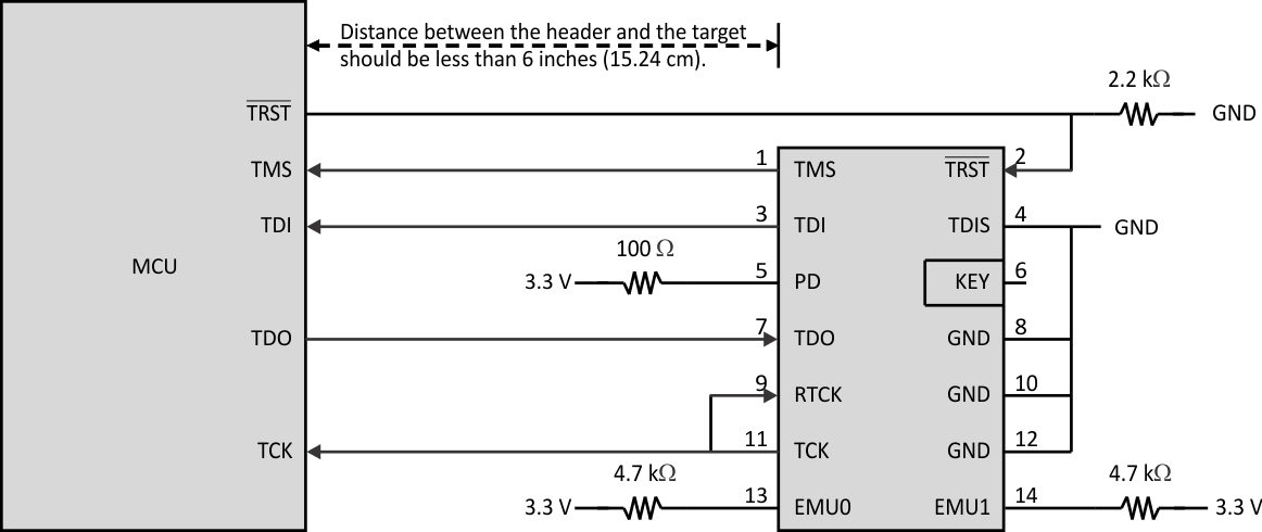 Figure 4-10 Connecting to the 14-Pin JTAG Header
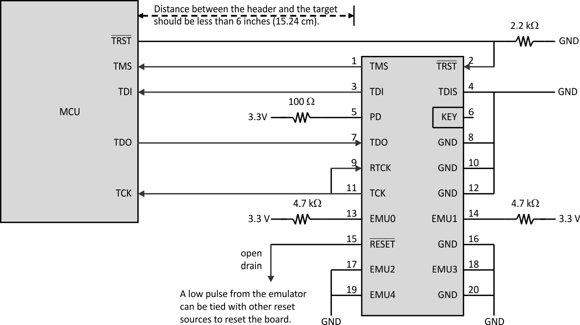 Figure 4-11 Connecting to the 20-Pin JTAG Header
4.7.5.1 JTAG Electrical Data and Timing
Table 4-21 lists the JTAG timing requirements. Table 4-22 lists the JTAG switching characteristics. Figure 4-12 shows the JTAG timing.
Table 4-21 JTAG Timing Requirements
| NO. | MIN | MAX | UNIT | ||
|---|---|---|---|---|---|
| 1 | tc(TCK) | Cycle time, TCK | 66.66 | ns | |
| 1a | tw(TCKH) | Pulse duration, TCK high (40% of tc) | 26.66 | ns | |
| 1b | tw(TCKL) | Pulse duration, TCK low (40% of tc) | 26.66 | ns | |
| 3 | tsu(TDI-TCKH) | Input setup time, TDI valid to TCK high | 13 | ns | |
| tsu(TMS-TCKH) | Input setup time, TMS valid to TCK high | 13 | ns | ||
| 4 | th(TCKH-TDI) | Input hold time, TDI valid from TCK high | 7 | ns | |
| th(TCKH-TMS) | Input hold time, TMS valid from TCK high | 7 | ns | ||
Table 4-22 JTAG Switching Characteristics
over recommended operating conditions (unless otherwise noted)| NO. | PARAMETER | MIN | MAX | UNIT | |
|---|---|---|---|---|---|
| 2 | td(TCKL-TDO) | Delay time, TCK low to TDO valid | 6 | 25 | ns |
 Figure 4-12 JTAG Timing
4.7.6 GPIO Electrical Data and Timing
The peripheral signals are multiplexed with general-purpose input/output (GPIO) signals. On reset, GPIO pins are configured as inputs. For specific inputs, the user can also select the number of input qualification cycles to filter unwanted noise glitches.
The GPIO module contains an Output X-BAR which allows an assortment of internal signals to be routed to a GPIO in the GPIO mux positions denoted as OUTPUTXBARx. The GPIO module also contains an Input X-BAR which is used to route signals from any GPIO input to different IP blocks such as the ADC(s), eCAP(s), ePWM(s), and external interrupts. For more details, see the X-BAR chapter in the TMS320F2837xD Dual-Core Delfino Microcontrollers Technical Reference Manual.
4.7.6.1 GPIO - Output Timing
Table 4-23 shows the general-purpose output switching characteristics. Figure 4-13 shows the general-purpose output timing.
Table 4-23 General-Purpose Output Switching Characteristics
over recommended operating conditions (unless otherwise noted)| PARAMETER | MIN | MAX | UNIT | ||
|---|---|---|---|---|---|
| tr(GPO) | Rise time, GPIO switching low to high | All GPIOs | 8(1) | ns | |
| tf(GPO) | Fall time, GPIO switching high to low | All GPIOs | 8(1) | ns | |
| tfGPO | Toggling frequency, GPO pins | 25 | MHz | ||
 Figure 4-13 General-Purpose Output Timing
4.7.6.2 GPIO - Input Timing
Table 4-24 shows the general-purpose input timing requirements. Figure 4-14 shows the sampling mode.
Table 4-24 General-Purpose Input Timing Requirements
| MIN | MAX | UNIT | |||
|---|---|---|---|---|---|
| tw(SP) | Sampling period | QUALPRD = 0 | 1tc(SYSCLK) | cycles | |
| QUALPRD ≠ 0 | 2tc(SYSCLK) * QUALPRD | cycles | |||
| tw(IQSW) | Input qualifier sampling window | tw(SP) * (n(1) – 1) | cycles | ||
| tw(GPI) (2) | Pulse duration, GPIO low/high | Synchronous mode | 2tc(SYSCLK) | cycles | |
| With input qualifier | tw(IQSW) + tw(SP) + 1tc(SYSCLK) | cycles | |||
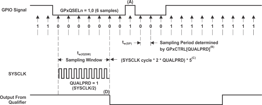
4.7.6.3 Sampling Window Width for Input Signals
The following section summarizes the sampling window width for input signals for various input qualifier configurations.
Sampling frequency denotes how often a signal is sampled with respect to SYSCLK.


In Equation 1, Equation 2, and Equation 3, SYSCLK cycle indicates the time period of SYSCLK.
Sampling period = SYSCLK cycle, if QUALPRD = 0
In a given sampling window, either 3 or 6 samples of the input signal are taken to determine the validity of the signal. This is determined by the value written to GPxQSELn register.
Case 1:
Qualification using 3 samples
Sampling window width = (SYSCLK cycle × 2 × QUALPRD) × 2, if QUALPRD ≠ 0
Sampling window width = (SYSCLK cycle) × 2, if QUALPRD = 0
Case 2:
Qualification using 6 samples
Sampling window width = (SYSCLK cycle × 2 × QUALPRD) × 5, if QUALPRD ≠ 0
Sampling window width = (SYSCLK cycle) × 5, if QUALPRD = 0
Figure 4-15 shows the general-purpose input timing.
 Figure 4-15 General-Purpose Input Timing
4.7.7 Interrupts
Figure 4-16 provides a high-level view of the interrupt architecture.
As shown in Figure 4-16, the devices support five external interrupts (XINT1 to XINT5) that can be mapped onto any of the GPIO pins.
In this device, 16 ePIE block interrupts are grouped into 1 CPU interrupt. In total, there are 12 CPU interrupt groups, with 16 interrupts per group.
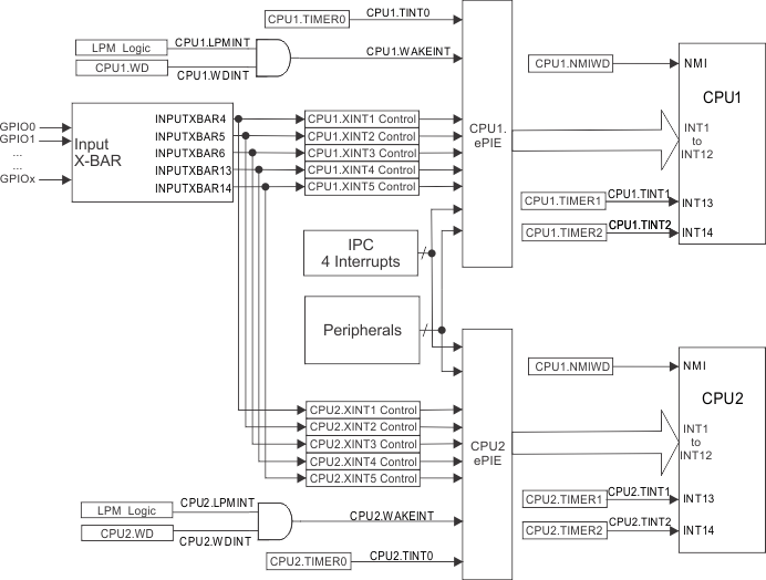 Figure 4-16 External and ePIE Interrupt Sources
4.7.7.1 External Interrupt (XINT) Electrical Data and Timing
Table 4-25 lists the external interrupt timing requirements. Table 4-26 lists the external interrupt switching characteristics. Figure 4-17 shows the external interrupt timing.
Table 4-25 External Interrupt Timing Requirements(1)
| MIN | MAX | UNIT | |||
|---|---|---|---|---|---|
| tw(INT) | Pulse duration, INT input low/high | Synchronous | 2tc(SYSCLK) | cycles | |
| With qualifier | tw(IQSW) + tw(SP) + 1tc(SYSCLK) | cycles | |||
Table 4-26 External Interrupt Switching Characteristics(1)
over recommended operating conditions (unless otherwise noted)| PARAMETER | MIN | MAX | UNIT | |
|---|---|---|---|---|
| td(INT) | Delay time, INT low/high to interrupt-vector fetch(2) | tw(IQSW) + 14tc(SYSCLK) | tw(IQSW) + tw(SP) + 14tc(SYSCLK) | cycles |
 Figure 4-17 External Interrupt Timing
4.7.8 Low-Power Modes
This device has three clock-gating low-power modes and a special power-gating mode.
Further details, as well as the entry and exit procedure, for all of the low-power modes can be found in the Low Power Modes section of the TMS320F2837xD Dual-Core Delfino Microcontrollers Technical Reference Manual.
4.7.8.1 Clock-Gating Low-Power Modes
IDLE, STANDBY, and HALT modes on this device are similar to those on other C28x devices. Table 4-27 describes the effect on the system when any of the clock-gating low-power modes are entered.
Table 4-27 Effect of Clock-Gating Low-Power Modes on the Device
| MODULES/ CLOCK DOMAIN |
CPU1 IDLE | CPU1 STANDBY | CPU2 IDLE | CPU2 STANDBY | HALT |
|---|---|---|---|---|---|
| CPU1.CLKIN | Active | Gated | N/A | N/A | Gated |
| CPU1.SYSCLK | Active | Gated | N/A | N/A | Gated |
| CPU1.CPUCLK | Gated | Gated | N/A | N/A | Gated |
| CPU2.CLKIN | N/A | N/A | Active | Gated | Gated |
| CPU2.SYSCLK | N/A | N/A | Active | Gated | Gated |
| CPU2.CPUCLK | N/A | N/A | Gated | Gated | Gated |
| Clock to modules Connected to PERx.SYSCLK | Active | Gated if CPUSEL.PERx = CPU1 | Active | Gated if CPUSEL.PERx = CPU2 | Gated |
| CPU1.WDCLK | Active | Active | N/A | N/A | Gated if CLKSRCCTL1.WDHALTI = 0 |
| CPU2.WDCLK | N/A | N/A | Active | Active | Gated |
| AUXPLLCLK | Active | Active | Active | Active | Gated |
| PLL | Powered | Powered | Powered | Powered | Software must power down PLL before entering HALT |
| INTOSC1 | Powered | Powered | Powered | Powered | Powered down if CLKSRCCTL1.WDHALTI = 0 |
| INTOSC2 | Powered | Powered | Powered | Powered | Powered down if CLKSRCCTL1.WDHALTI = 0 |
| Flash | Powered | Powered | Powered | Powered | Software-Controlled |
| X1/X2 Crystal Oscillator | Powered | Powered | Powered | Powered | Powered-Down |
4.7.8.2 Power-Gating Low-Power Modes
HIBERNATE mode is the lowest power mode on this device. It is a global low-power mode that gates the supply voltages to most of the system. HIBERNATE is essentially a controlled power-down with remote wakeup capability, and can be used to save power during long periods of inactivity. Table 4-28 describes the effects on the system when the HIBERNATE mode is entered.
Table 4-28 Effect of Power-Gating Low-Power Mode on the Device
| MODULES/POWER DOMAINS | HIBERNATE |
|---|---|
| M0 and M1 memories | ● Remain on with memory retention if LPMCR.M0M1MODE = 0x00 ● Are off when LPMCR.M0M1MODE = 0x01 |
| CPU1, CPU2 digital peripherals | Powered down |
| Dx, LSx, GSx memories | Power down, memory contents are lost |
| I/Os | On with output state preserved |
| Oscillators, PLL, analog peripherals, Flash | Enters Low-Power Mode |
4.7.8.3 Low-Power Mode Wakeup Timing
Table 4-29 shows the IDLE mode timing requirements, Table 4-30 shows the switching characteristics, and Figure 4-18 shows the timing diagram for IDLE mode.
Table 4-29 IDLE Mode Timing Requirements(1)
| MIN | MAX | UNIT | ||||
|---|---|---|---|---|---|---|
| tw(WAKE) | Pulse duration, external wake-up signal | Without input qualifier | 2tc(SYSCLK) | cycles | ||
| With input qualifier | 2tc(SYSCLK) + tw(IQSW) | |||||
Table 4-30 IDLE Mode Switching Characteristics(1)
over recommended operating conditions (unless otherwise noted)| PARAMETER | TEST CONDITIONS | MIN | MAX | UNIT | |
|---|---|---|---|---|---|
| td(WAKE-IDLE) | Delay time, external wake signal to program execution resume (2) | cycles | |||
|
Without input qualifier | 40tc(SYSCLK) | |||
| With input qualifier | 40tc(SYSCLK) + tw(WAKE) | ||||
|
Without input qualifier | 6700tc(SYSCLK)(3) | |||
| With input qualifier | 6700tc(SYSCLK)(3) + tw(WAKE) | ||||
|
Without input qualifier | 25tc(SYSCLK) | |||
| With input qualifier | 25tc(SYSCLK) + tw(WAKE) | ||||

Table 4-31 shows the STANDBY mode timing requirements, Table 4-32 shows the switching characteristics, and Figure 4-19 shows the timing diagram for STANDBY mode.
Table 4-31 STANDBY Mode Timing Requirements
| MIN | MAX | UNIT | ||||
|---|---|---|---|---|---|---|
| tw(WAKE-INT) | Pulse duration, external wake-up signal | QUALSTDBY = 0 | 2tc(OSCCLK) | 3tc(OSCCLK) | cycles | ||
| QUALSTDBY > 0 | (2 + QUALSTDBY)tc(OSCCLK)(1) |
(2 + QUALSTDBY) * tc(OSCCLK) | |||||
Table 4-32 STANDBY Mode Switching Characteristics
over recommended operating conditions (unless otherwise noted)| PARAMETER | TEST CONDITIONS | MIN | MAX | UNIT | |
|---|---|---|---|---|---|
| td(IDLE-XCOS) | Delay time, IDLE instruction executed to XCLKOUT stop | 16tc(INTOSC1) | cycles | ||
| td(WAKE-STBY) | Delay time, external wake signal to program execution resume(1) | cycles | |||
|
175tc(SYSCLK) + tw(WAKE-INT) | ||||
|
6700tc(SYSCLK)(2) + tw(WAKE-INT) | ||||
|
3tc(OSC) + 15tc(SYSCLK) + tw(WAKE-INT) | ||||
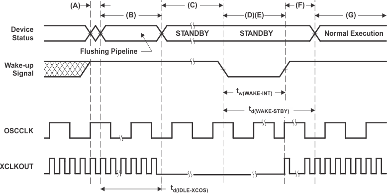
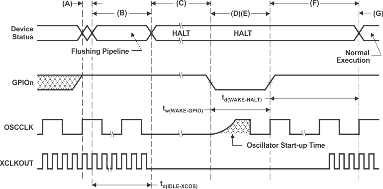
Table 4-33 shows the HALT mode timing requirements, Table 4-34 shows the switching characteristics, and Figure 4-20 shows the timing diagram for HALT mode.
Table 4-33 HALT Mode Timing Requirements
| MIN | MAX | UNIT | |||
|---|---|---|---|---|---|
| tw(WAKE-GPIO) | Pulse duration, GPIO wake-up signal(1) | toscst + 2tc(OSCCLK) | cycles | ||
| tw(WAKE-XRS) | Pulse duration, XRS wake-up signal(1) | toscst + 8tc(OSCCLK) | cycles | ||
Table 4-34 HALT Mode Switching Characteristics
over recommended operating conditions (unless otherwise noted)| PARAMETER | MIN | MAX | UNIT | |
|---|---|---|---|---|
| td(IDLE-XCOS) | Delay time, IDLE instruction executed to XCLKOUT stop | 16tc(INTOSC1) | cycles | |
| td(WAKE-HALT) | Delay time, external wake signal end to CPU1 program execution resume | cycles | ||
|
75tc(OSCCLK) | |||
|
17500tc(OSCCLK) (1) | |||
|
75tc(OSCCLK) | |||
NOTE
CPU2 should enter IDLE mode before CPU1 puts the device into HALT mode. CPU1 should verify that CPU2 has entered IDLE mode using the LPMSTAT register before calling the IDLE instruction to enter HALT.
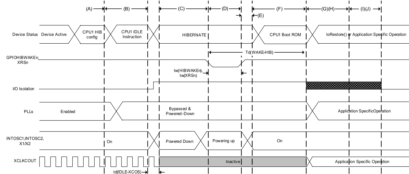
Table 4-35 shows the HIBERNATE mode timing requirements, Table 4-36 shows the switching characteristics, and Figure 4-21 shows the timing diagram for HIBERNATE mode.
Table 4-35 HIBERNATE Mode Timing Requirements
| MIN | MAX | UNIT | ||
|---|---|---|---|---|
| tw(HIBWAKE) | Pulse duration, HIBWAKE signal | 40 | µs | |
| tw(WAKEXRS) | Pulse duration, XRS wake-up signal | 40 | µs | |
Table 4-36 HIBERNATE Mode Switching Characteristics
over recommended operating conditions (unless otherwise noted)| PARAMETER | MIN | MAX | UNIT | |
|---|---|---|---|---|
| td(IDLE-XCOS) | Delay time, IDLE instruction executed to XCLKOUT stop | 30tc(SYSCLK) | cycles | |
| td(WAKE-HIB) | Delay time, external wake signal to lORestore function start | 1.5 | ms | |
NOTE
- If the IORESTOREADDR is configured as the default value, the BootROM will continue its execution to boot as determined by the HIBBOOTMODE register. Refer to the ROM Code and Peripheral Booting chapter of the TMS320F2837xD Dual-Core Delfino Microcontrollers Technical Reference Manual for more information.
- The user may choose to disable I/O Isolation at any point in the IoRestore function. Regardless if the user has disabled Isolation in the IoRestore function or if IoRestore is not defined, the BootROM will automatically disable isolation before booting as determined by the HIBBOOTMODE register.
NOTE
For applications using both CPU1 and CPU2, TI recommends that the application puts CPU2 in either IDLE or STANDBY before entering HIBERNATE mode. If any GPIOs are used and the state is to be preserved, data can be stored in M0/M1 memory of CPU1 to be reconfigured upon wakeup. This should be done before step A of Figure 4-21.
4.7.9 External Memory Interface (EMIF)
The EMIF provides a means of connecting the CPU to various external storage devices like asynchronous memories (SRAM, NOR flash) or synchronous memory (SDRAM).
4.7.9.1 Asynchronous Memory Support
The EMIF supports asynchronous memories:
- SRAMs
- NOR Flash memories
There is an external wait input that allows slower asynchronous memories to extend the memory access. The EMIF module supports up to three chip selects (EMIF_CS[4:2]). Each chip select has the following individually programmable attributes:
- Data bus width
- Read cycle timings: setup, hold, strobe
- Write cycle timings: setup, hold, strobe
- Bus turnaround time
- Extended wait option with programmable time-out
- Select strobe option
4.7.9.2 Synchronous DRAM Support
The EMIF memory controller is compliant with the JESD21-C SDR SDRAMs that use a 32-bit or 16-bit data bus. The EMIF has a single SDRAM chip select (EMIF_CS[0]).
The address space of the EMIF, for the synchronous memory (SDRAM), lies beyond the 22-bit range of the program address bus and can only be accessed through the data bus, which places a restriction on the C compiler being able to work effectively on data in this space. Therefore, when using SDRAM, the user is advised to copy data (using the DMA) from external memory to RAM before working on it. See the examples in controlSUITE™ (CONTROLSUITE) and the TMS320F2837xD Dual-Core Delfino Microcontrollers Technical Reference Manual.
SDRAM configurations supported are:
- One-bank, two-bank, and four-bank SDRAM devices
- Devices with 8-, 9-, 10-, and 11-column addresses
- CAS latency of two or three clock cycles
- 16-bit/32-bit data bus width
- 3.3-V LVCMOS interface
Additionally, the EMIF supports placing the SDRAM in self-refresh and power-down modes. Self-refresh mode allows the SDRAM to be put in a low-power state while still retaining memory contents because the SDRAM will continue to refresh itself even without clocks from the microcontroller. Power-down mode achieves even lower power, except the microcontroller must periodically wake up and issue refreshes if data retention is required. The EMIF module does not support mobile SDRAM devices.
On this device, the EMIF does not support burst access for SDRAM configurations. This means every access to an external SDRAM device will have CAS latency.
4.7.9.3 EMIF Electrical Data and Timing
4.7.9.3.1 Asynchronous RAM
Table 4-37 shows the EMIF asynchronous memory timing requirements. Table 4-38 shows the EMIF asynchronous memory switching characteristics. Figure 4-22 through Figure 4-25 show the EMIF asynchronous memory timing diagrams.
Table 4-37 EMIF Asynchronous Memory Timing Requirements(1)
| NO. | MIN | MAX | UNIT | ||
|---|---|---|---|---|---|
| Reads and Writes | |||||
| E | EMIF clock period | tc(SYSCLK) | ns | ||
| 2 | tw(EM_WAIT) | Pulse duration, EMxWAIT assertion and deassertion | 2E | ns | |
| Reads | |||||
| 12 | tsu(EMDV-EMOEH) | Setup time, EMxD[y:0] valid before EMxOE high | 15 | ns | |
| 13 | th(EMOEH-EMDIV) | Hold time, EMxD[y:0] valid after EMxOE high | 0 | ns | |
| 14 | tsu(EMOEL-EMWAIT) | Setup Time, EMxWAIT asserted before end of Strobe Phase(2) | 4E+20 | ns | |
| Writes | |||||
| 28 | tsu(EMWEL-EMWAIT) | Setup Time, EMxWAIT asserted before end of Strobe Phase(2) | 4E+20 | ns | |
Table 4-38 EMIF Asynchronous Memory Switching Characteristics(1)(2)(3)
| NO. | PARAMETER | MIN | MAX | UNIT | |
|---|---|---|---|---|---|
| Reads and Writes | |||||
| 1 | td(TURNAROUND) | Turn around time | (TA)*E–3 | (TA)*E+2 | ns |
| Reads | |||||
| 3 | tc(EMRCYCLE) | EMIF read cycle time (EW = 0) | (RS+RST+RH+2)*E–3 | (RS+RST+RH+2)*E+2 | ns |
| EMIF read cycle time (EW = 1) | (RS+RST+RH+2+ (EWC*16))*E–3 |
(RS+RST+RH+2+ (EWC*16))*E+2 |
ns | ||
| 4 | tsu(EMCEL-EMOEL) | Output setup time, EMxCS[y:2] low to EMxOE low (SS = 0) | (RS)*E–3 | (RS)*E+2 | ns |
| Output setup time, EMxCS[y:2] low to EMxOE low (SS = 1) | –3 | 2 | ns | ||
| 5 | th(EMOEH-EMCEH) | Output hold time, EMxOE high to EMxCS[y:2] high (SS = 0) | (RH)*E–3 | (RH)*E | ns |
| Output hold time, EMxOE high to EMxCS[y:2] high (SS = 1) | –3 | 0 | ns | ||
| 6 | tsu(EMBAV-EMOEL) | Output setup time, EMxBA[y:0] valid to EMxOE low | (RS)*E–3 | (RS)*E+2 | ns |
| 7 | th(EMOEH-EMBAIV) | Output hold time, EMxOE high to EMxBA[y:0] invalid | (RH)*E–3 | (RH)*E | ns |
| 8 | tsu(EMAV-EMOEL) | Output setup time, EMxA[y:0] valid to EMxOE low | (RS)*E–3 | (RS)*E+2 | ns |
| 9 | th(EMOEH-EMAIV) | Output hold time, EMxOE high to EMxA[y:0] invalid | (RH)*E–3 | (RH)*E | ns |
| 10 | tw(EMOEL) | EMxOE active low width (EW = 0) | (RST)*E–1 | (RST)*E+1 | ns |
| EMxOE active low width (EW = 1) | (RST+(EWC*16))*E–1 | (RST+(EWC*16))*E+1 | ns | ||
| 11 | td(EMWAITH-EMOEH) | Delay time from EMxWAIT deasserted to EMxOE high | 4E+10 | 5E+15 | ns |
| 29 | tsu(EMDQMV-EMOEL) | Output setup time, EMxDQM[y:0] valid to EMxOE low | (RS)*E–3 | (RS)*E+2 | ns |
| 30 | th(EMOEH-EMDQMIV) | Output hold time, EMxOE high to EMxDQM[y:0] invalid | (RH)*E–3 | (RH)*E | ns |
| Writes | |||||
| 15 | tc(EMWCYCLE) | EMIF write cycle time (EW = 0) | (WS+WST+WH+2)*E–3 | (WS+WST+WH+2)*E+1 | ns |
| EMIF write cycle time (EW = 1) | (WS+WST+WH+2+ (EWC*16))*E–3 |
(WS+WST+WH+2+ (EWC*16))*E+1 |
ns | ||
| 16 | tsu(EMCEL-EMWEL) | Output setup time, EMxCS[y:2] low to EMxWE low (SS = 0) | (WS)*E–3 | (WS)*E+1 | ns |
| Output setup time, EMxCS[y:2] low to EMxWE low (SS = 1) | –3 | 1 | ns | ||
| 17 | th(EMWEH-EMCEH) | Output hold time, EMxWE high to EMxCS[y:2] high (SS = 0) | (WH)*E–3 | (WH)*E | ns |
| Output hold time, EMxWE high to EMxCS[y:2] high (SS = 1) | –3 | 0 | ns | ||
| 18 | tsu(EMDQMV-EMWEL) | Output setup time, EMxDQM[y:0] valid to EMxWE low | (WS)*E–3 | (WS)*E+1 | ns |
| 19 | th(EMWEH-EMDQMIV) | Output hold time, EMxWE high to EMxDQM[y:0] invalid | (WH)*E–3 | (WH)*E | ns |
| 20 | tsu(EMBAV-EMWEL) | Output setup time, EMxBA[y:0] valid to EMxWE low | (WS)*E–3 | (WS)*E+1 | ns |
| 21 | th(EMWEH-EMBAIV) | Output hold time, EMxWE high to EMxBA[y:0] invalid | (WH)*E–3 | (WH)*E | ns |
| 22 | tsu(EMAV-EMWEL) | Output setup time, EMxA[y:0] valid to EMxWE low | (WS)*E–3 | (WS)*E+1 | ns |
| 23 | th(EMWEH-EMAIV) | Output hold time, EMxWE high to EMxA[y:0] invalid | (WH)*E–3 | (WH)*E | ns |
| 24 | tw(EMWEL) | EMxWE active low width (EW = 0) |
(WST)*E–1 | (WST)*E+1 | ns |
| EMxWE active low width (EW = 1) |
(WST+(EWC*16))*E–1 | (WST+(EWC*16))*E+1 | ns | ||
| 25 | td(EMWAITH-EMWEH) | Delay time from EMxWAIT deasserted to EMxWE high | 4E+10 | 5E+15 | ns |
| 26 | tsu(EMDV-EMWEL) | Output setup time, EMxD[y:0] valid to EMxWE low | (WS)*E–3 | (WS)*E+1 | ns |
| 27 | th(EMWEH-EMDIV) | Output hold time, EMxWE high to EMxD[y:0] invalid | (WH)*E–3 | (WH)*E | ns |
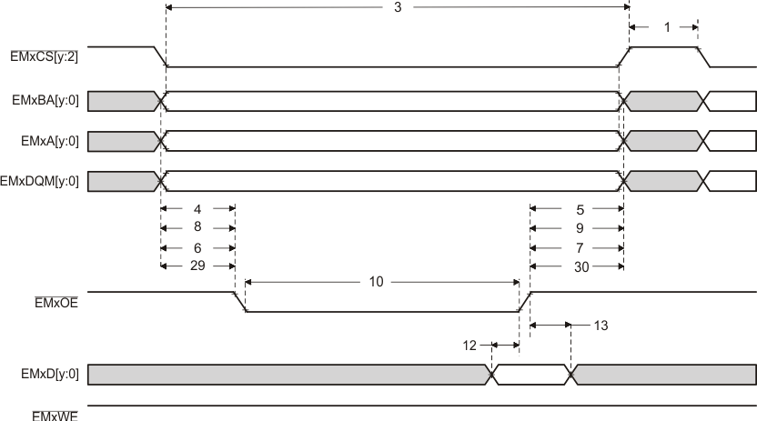 Figure 4-22 Asynchronous Memory Read Timing
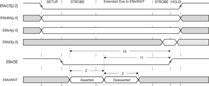 Figure 4-23 EMxWAIT Read Timing Requirements
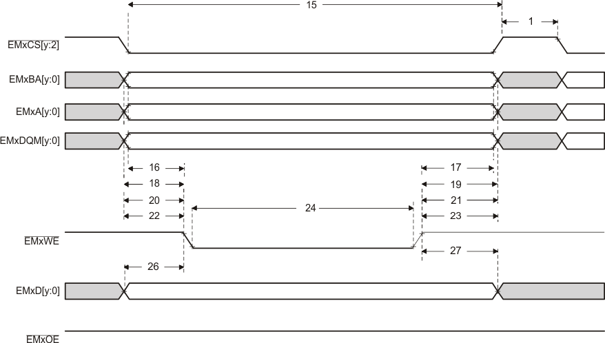 Figure 4-24 Asynchronous Memory Write Timing
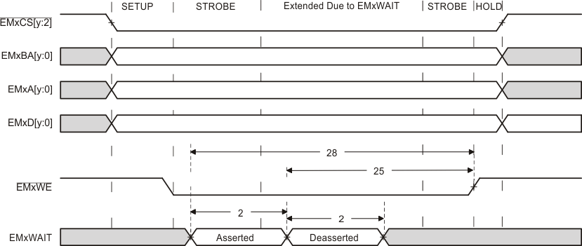 Figure 4-25 EMxWAIT Write Timing Requirements
4.7.9.3.2 Synchronous RAM
Table 4-39 shows the EMIF synchronous memory timing requirements. Table 4-40 shows the EMIF synchronous memory switching characteristics. Figure 4-26 and Figure 4-27 show the synchronous memory timing diagrams.
Table 4-39 EMIF Synchronous Memory Timing Requirements
| NO. | MIN | MAX | UNIT | ||
|---|---|---|---|---|---|
| 19 | tsu(EMIFDV-EM_CLKH) | Input setup time, read data valid on EMxD[y:0] before EMxCLK rising | 2 | ns | |
| 20 | th(CLKH-DIV) | Input hold time, read data valid on EMxD[y:0] after EMxCLK rising | 1.5 | ns | |
Table 4-40 EMIF Synchronous Memory Switching Characteristics
| NO. | PARAMETER | MIN | MAX | UNIT | |
|---|---|---|---|---|---|
| 1 | tc(CLK) | Cycle time, EMIF clock EMxCLK | 10 | ns | |
| 2 | tw(CLK) | Pulse width, EMIF clock EMxCLK high or low | 3 | ns | |
| 3 | td(CLKH-CSV) | Delay time, EMxCLK rising to EMxCS[y:2] valid | 8 | ns | |
| 4 | toh(CLKH-CSIV) | Output hold time, EMxCLK rising to EMxCS[y:2] invalid | 1 | ns | |
| 5 | td(CLKH-DQMV) | Delay time, EMxCLK rising to EMxDQM[y:0] valid | 8 | ns | |
| 6 | toh(CLKH-DQMIV) | Output hold time, EMxCLK rising to EMxDQM[y:0] invalid | 1 | ns | |
| 7 | td(CLKH-AV) | Delay time, EMxCLK rising to EMxA[y:0] and EMxBA[y:0] valid | 8 | ns | |
| 8 | toh(CLKH-AIV) | Output hold time, EMxCLK rising to EMxA[y:0] and EMxBA[y:0] invalid | 1 | ns | |
| 9 | td(CLKH-DV) | Delay time, EMxCLK rising to EMxD[y:0] valid | 8 | ns | |
| 10 | toh(CLKH-DIV) | Output hold time, EMxCLK rising to EMxD[y:0] invalid | 1 | ns | |
| 11 | td(CLKH-RASV) | Delay time, EMxCLK rising to EMxRAS valid | 8 | ns | |
| 12 | toh(CLKH-RASIV) | Output hold time, EMxCLK rising to EMxRAS invalid | 1 | ns | |
| 13 | td(CLKH-CASV) | Delay time, EMxCLK rising to EMxCAS valid | 8 | ns | |
| 14 | toh(CLKH-CASIV) | Output hold time, EMxCLK rising to EMxCAS invalid | 1 | ns | |
| 15 | td(CLKH-WEV) | Delay time, EMxCLK rising to EMxWE valid | 8 | ns | |
| 16 | toh(CLKH-WEIV) | Output hold time, EMxCLK rising to EMxWE invalid | 1 | ns | |
| 17 | td(CLKH-DHZ) | Delay time, EMxCLK rising to EMxD[y:0] tri-stated | 8 | ns | |
| 18 | toh(CLKH-DLZ) | Output hold time, EMxCLK rising to EMxD[y:0] driving | 1 | ns | |
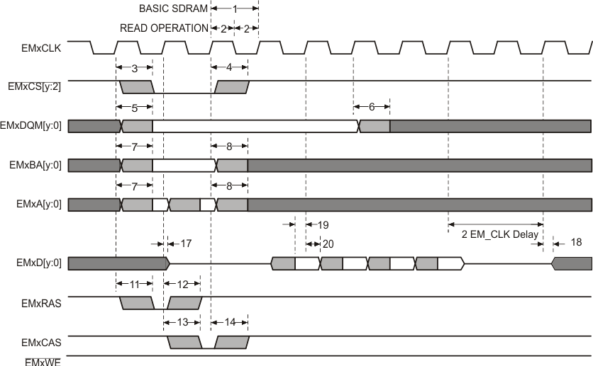 Figure 4-26 Basic SDRAM Read Operation
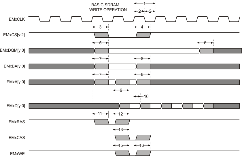 Figure 4-27 Basic SDRAM Write Operation
4.8 Analog Peripherals
This analog subsystem module is described in this section.
The analog modules on this device include the ADC, temperature sensor, buffered DAC, and CMPSS.
The analog subsystem has the following features:
- Flexible voltage references
- VREFHIA and VREFLOA, VREFHIB and VREFLOB, VREFHIC and VREFLOC, and VREFHID and VREFLOD externally supplied reference voltage pins
- Selectable by ADCs and buffered DACs
- VDAC externally supplied reference voltage pin
- Selectable by buffered DACs and comparator subsystem DACs
- Low reference is VSSA
- VREFHIA and VREFLOA, VREFHIB and VREFLOB, VREFHIC and VREFLOC, and VREFHID and VREFLOD externally supplied reference voltage pins
- Flexible pin usage
- Buffered DAC and comparator subsystem functions multiplexed with ADC inputs
- Internal connection to VREFLO on all ADCs for offset self-calibration
Figure 4-28 shows the Analog Subsystem Block Diagram for the 337-ball ZWT package. Figure 4-29 shows the Analog Subsystem Block Diagram for the 176-pin PTP package. Figure 4-30 shows the Analog Subsystem Block Diagram for the 100-pin PZP package.
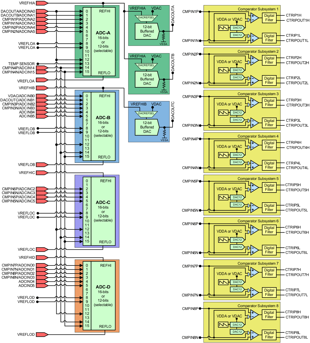 Figure 4-28 Analog Subsystem Block Diagram (337-Ball ZWT)
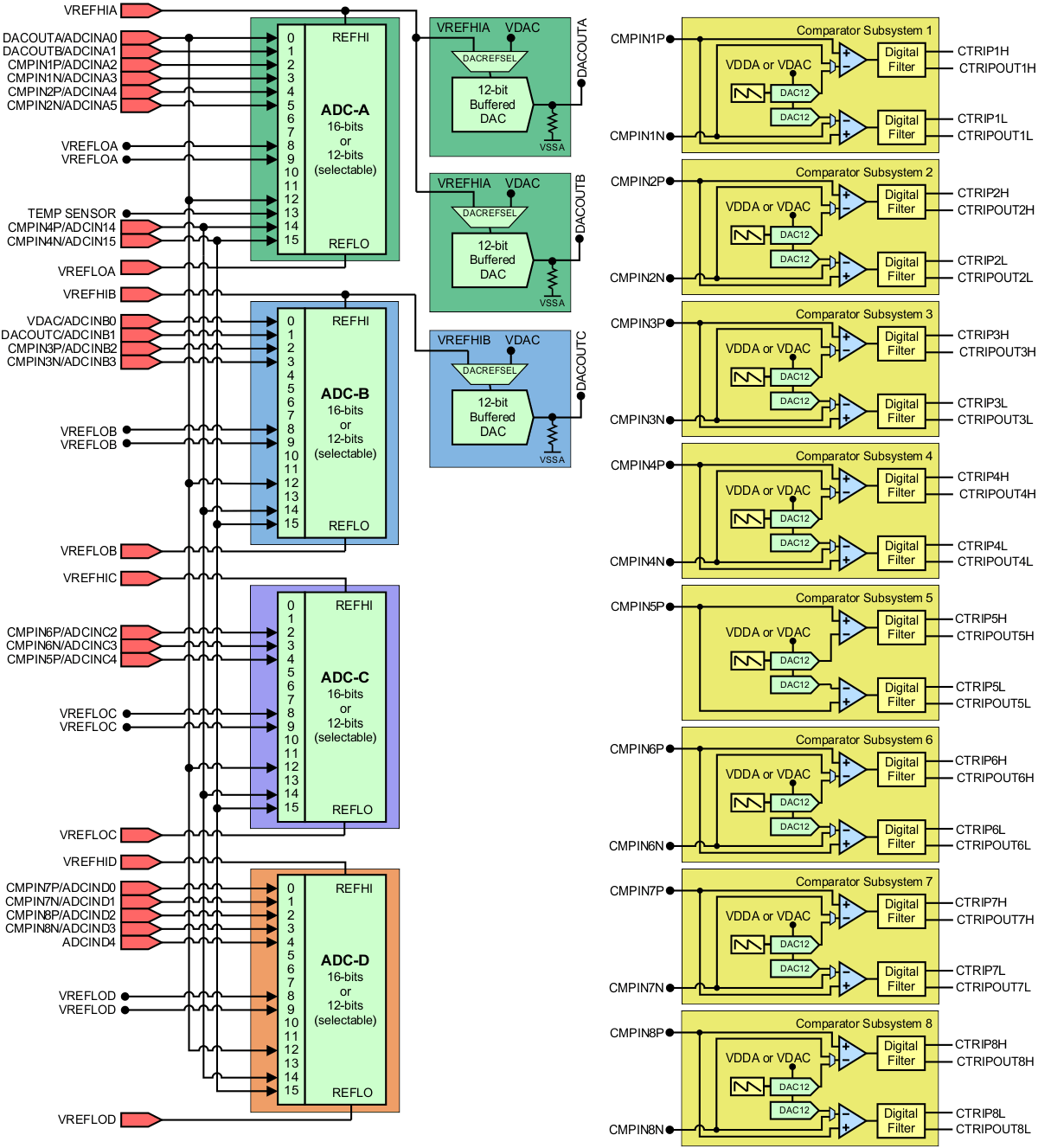 Figure 4-29 Analog Subsystem Block Diagram (176-Pin PTP)
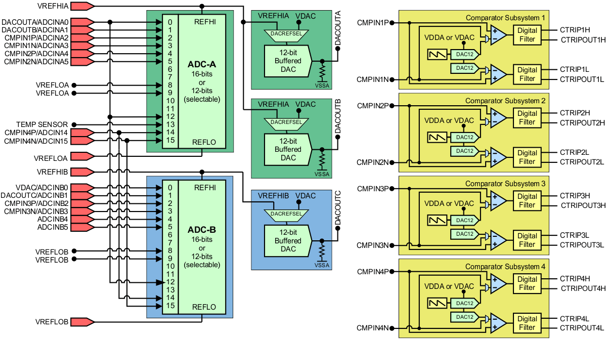 Figure 4-30 Analog Subsystem Block Diagram (100-Pin PZP)
4.8.1 Analog-to-Digital Converter (ADC)
The ADCs on this device are successive approximation (SAR) style ADCs with selectable resolution of either 16 bits or 12 bits. There are multiple ADC modules which allow simultaneous sampling. The ADC wrapper is start-of-conversion (SOC) based [see the SOC Principle of Operation section of the TMS320F2837xD Dual-Core Delfino Microcontrollers Technical Reference Manual.
Each ADC has the following features:
- Selectable resolution of 16 bits or 12 bits
- Ratiometric external reference set by VREFHI and VREFLO
- Differential signal conversions (16-bit mode only)
- Single-ended signal conversions (12-bit mode only)
- Input multiplexer with up to 16 channels (single-ended) or 8 channels (differential)
- 16 configurable SOCs
- 16 individually addressable result registers
- Multiple trigger sources
- Software immediate start
- All ePWMs
- GPIO XINT2
- CPU timers
- ADCINT1 or 2
- Four flexible PIE interrupts
- Burst mode
- Four post-processing blocks, each with:
- Saturating offset calibration
- Error from setpoint calculation
- High, low, and zero-crossing compare, with interrupt and ePWM trip capability
- Trigger-to-sample delay capture
Figure 4-31 shows the ADC module block diagram.
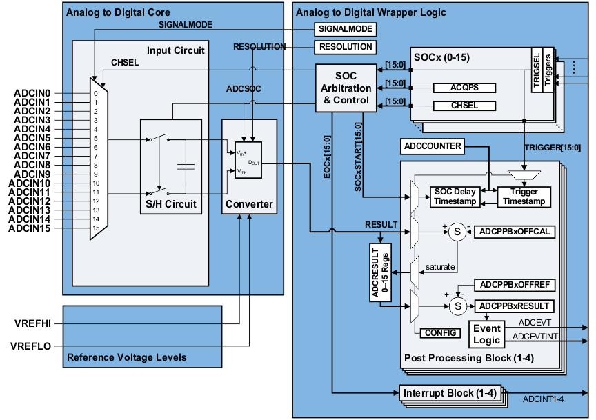 Figure 4-31 ADC Module Block Diagram
4.8.1.1 ADC Electrical Data and Timing
Table 4-41 shows the ADC operating conditions for 16-bit differential mode. Table 4-42 shows the ADC characteristics for 16-bit differential mode. Table 4-43 shows the ADC operating conditions for 12-bit single-ended mode. Table 4-44 shows the ADC characteristics for 12-bit single-ended mode. Table 4-45 shows the ADCEXTSOC timing requirements.
Table 4-41 ADC Operating Conditions (16-Bit Differential Mode)
over recommended operating conditions (unless otherwise noted)| MIN | TYP | MAX | UNIT | ||
|---|---|---|---|---|---|
| ADCCLK (derived from PERx.SYSCLK) | 5 | 50 | MHz | ||
| Sample window duration (set by ACQPS and PERx.SYSCLK)(1) | 320 | ns | |||
| VREFHI | 2.4 | 2.5 or 3.0 | VDDA | V | |
| VREFLO | VSSA | 0 | VSSA | V | |
| VREFHI – VREFLO | 2.4 | VDDA | V | ||
| ADC input conversion range | VREFLO | VREFHI | V | ||
| ADC input signal common mode voltage(2)(3) | VREFCM – 50 | VREFCM | VREFCM + 50 | mV | |
NOTE
The ADC inputs should be kept below VDDA + 0.3 V during operation. If an ADC input exceeds this level, the VREF internal to the device may be disturbed, which can impact results for other ADC or DAC inputs using the same VREF.
Table 4-42 ADC Characteristics (16-Bit Differential Mode)
over recommended operating conditions (unless otherwise noted)(6)| PARAMETER | TEST CONDITIONS | MIN | TYP | MAX | UNIT |
|---|---|---|---|---|---|
| ADC conversion cycles(1) | 29.6 | 31 | ADCCLKs | ||
| Power-up time (after setting ADCPWDNZ to first conversion) | 500 | µs | |||
| Gain error | –64 | ±9 | 64 | LSBs | |
| Offset error(2) | –16 | ±9 | 16 | LSBs | |
| Channel-to-channel gain error | ±6 | LSBs | |||
| Channel-to-channel offset error | ±3 | LSBs | |||
| ADC-to-ADC gain error | Identical VREFHI and VREFLO for all ADCs | ±6 | LSBs | ||
| ADC-to-ADC offset error | Identical VREFHI and VREFLO for all ADCs | ±3 | LSBs | ||
| DNL(3) | > –1 | ±0.5 | 1 | LSBs | |
| INL | –3 | ±1.5 | 3 | LSBs | |
| SNR(4)(11) | VREFHI = 2.5 V, fin = 10 kHz | 87.6 | dB | ||
| THD(4)(11) | VREFHI = 2.5 V, fin = 10 kHz | –93.5 | dB | ||
| SFDR(4)(11) | VREFHI = 2.5 V, fin = 10 kHz | 95.4 | dB | ||
| SINAD(4)(11) | VREFHI = 2.5 V, fin = 10 kHz | 86.6 | dB | ||
| ENOB(4)(11) | VREFHI = 2.5 V, fin = 10 kHz, single ADC(7) |
14.1 | bits | ||
| VREFHI = 2.5 V, fin = 10 kHz, synchronous ADCs(8) | 14.1 | ||||
| VREFHI = 2.5 V, fin = 10 kHz, asynchronous ADCs(9) | Not supported | ||||
| PSRR | VDDA = 3.3-V DC + 200 mV DC up to Sine at 1 kHz |
77 | dB | ||
| PSRR | VDDA = 3.3-V DC + 200 mV Sine at 800 kHz |
74 | dB | ||
| CMRR | DC to 1 MHz | 60 | dB | ||
| VREFHI input current | 190 | µA | |||
| ADC-to-ADC isolation(11)(5)(10) | VREFHI = 2.5 V, synchronous ADCs(8) | –2 | 2 | LSBs | |
| VREFHI = 2.5 V, asynchronous ADCs(9) | Not supported |
Table 4-43 ADC Operating Conditions (12-Bit Single-Ended Mode)
over recommended operating conditions (unless otherwise noted)| MIN | TYP | MAX | UNIT | |
|---|---|---|---|---|
| ADCCLK (derived from PERx.SYSCLK) | 5 | 50 | MHz | |
| Sample window duration (set by ACQPS and PERx.SYSCLK)(1) | 75 | ns | ||
| VREFHI | 2.4 | 2.5 or 3.0 | VDDA | V |
| VREFLO | VSSA | 0 | VSSA | V |
| VREFHI – VREFLO | 2.4 | VDDA | V | |
| ADC input conversion range | VREFLO | VREFHI | V |
NOTE
The ADC inputs should be kept below VDDA + 0.3 V during operation. If an ADC input exceeds this level, the VREF internal to the device may be disturbed, which can impact results for other ADC or DAC inputs using the same VREF.
Table 4-44 ADC Characteristics (12-Bit Single-Ended Mode)
over recommended operating conditions (unless otherwise noted)(5)| PARAMETER | TEST CONDITIONS | MIN | TYP | MAX | UNIT |
|---|---|---|---|---|---|
| ADC conversion cycles(1) | 10.1 | 11 | ADCCLKs | ||
| Power-up time | 500 | µs | |||
| Gain error | –5 | ±3 | 5 | LSBs | |
| Offset error | –4 | ±2 | 4 | LSBs | |
| Channel-to-channel gain error | ±4 | LSBs | |||
| Channel-to-channel offset error | ±2 | LSBs | |||
| ADC-to-ADC gain error | Identical VREFHI and VREFLO for all ADCs | ±4 | LSBs | ||
| ADC-to-ADC offset error | Identical VREFHI and VREFLO for all ADCs | ±2 | LSBs | ||
| DNL(2) | > –1 | ±0.5 | 1 | LSBs | |
| INL | –2 | ±1.0 | 2 | LSBs | |
| SNR(3)(10) | VREFHI = 2.5 V, fin = 100 kHz | 68.8 | dB | ||
| THD(3)(10) | VREFHI = 2.5 V, fin = 100 kHz | –78.4 | dB | ||
| SFDR(3)(10) | VREFHI = 2.5 V, fin = 100 kHz | 79.2 | dB | ||
| SINAD(3)(10) | VREFHI = 2.5 V, fin = 100 kHz | 68.4 | dB | ||
| ENOB(3)(10) | VREFHI = 2.5 V, fin = 100 kHz, single ADC(6), all packages |
11.1 | bits | ||
| VREFHI = 2.5 V, fin = 100 kHz, synchronous ADCs(7), all packages | 11.1 | ||||
| VREFHI = 2.5 V, fin = 100 kHz, asynchronous ADCs(8), 100-pin PZP package |
Not supported | ||||
| VREFHI = 2.5 V, fin = 100 kHz, asynchronous ADCs(8), 176-pin PTP package |
9.7 | ||||
| VREFHI = 2.5 V, fin = 100 kHz, asynchronous ADCs(8), 337-ball ZWT package |
10.9 | ||||
| PSRR | VDDA = 3.3-V DC + 200 mV DC up to Sine at 1 kHz |
60 | dB | ||
| PSRR | VDDA = 3.3-V DC + 200 mV Sine at 800 kHz |
57 | dB | ||
| ADC-to-ADC isolation(10)(4)(9) | VREFHI = 2.5 V, synchronous ADCs(7), all packages | –1 | 1 | LSBs | |
| VREFHI = 2.5 V, asynchronous ADCs(8), 100-pin PZP package | Not supported | ||||
| VREFHI = 2.5 V, asynchronous ADCs(8), 176-pin PTP package | –9 | 9 | |||
| VREFHI = 2.5 V, asynchronous ADCs(8), 337-ball ZWT package | –2 | 2 | |||
| VREFHI input current | 130 | µA |
Table 4-45 ADCEXTSOC Timing Requirements(1)
| MIN | MAX | UNIT | |||
|---|---|---|---|---|---|
| tw(INT) | Pulse duration, INT input low/high | Synchronous | 2tc(SYSCLK) | cycles | |
| With qualifier | tw(IQSW) + tw(SP) + 1tc(SYSCLK) | cycles | |||
4.8.1.1.1 ADC Input Models
NOTE
ADC channels ADCINA0, ADCINA1, and ADCINB1 have a 50-kΩ pulldown resistor to VSSA.
For single-ended operation, the ADC input characteristics are given by Table 4-46 and Figure 4-32.
Table 4-46 Single-Ended Input Model Parameters
| DESCRIPTION | VALUE (12-BIT MODE) | |
|---|---|---|
| Cp | Parasitic input capacitance | See Table 4-48 |
| Ron | Sampling switch resistance | 425 Ω |
| Ch | Sampling capacitor | 14.5 pF |
| Rs | Nominal source impedance | 50 Ω |
 Figure 4-32 Single-Ended Input Model
For differential operation, the ADC input characteristics are given by Table 4-47 and Figure 4-33.
Table 4-47 Differential Input Model Parameters
| DESCRIPTION | VALUE (16-BIT MODE) | |
|---|---|---|
| Cp | Parasitic input capacitance | See Table 4-48 |
| Ron | Sampling switch resistance | 700 Ω |
| Ch | Sampling capacitor | 16.5 pF |
| Rs | Nominal source impedance | 50 Ω |
 Figure 4-33 Differential Input Model
Table 4-48 shows the parasitic capacitance on each channel. Also, enabling a comparator adds approximately 1.4 pF of capacitance on positive comparator inputs and 2.5 pF of capacitance on negative comparator inputs.
Table 4-48 Per-Channel Parasitic Capacitance
| ADC CHANNEL | Cp (pF) | |
|---|---|---|
| COMPARATOR DISABLED | COMPARATOR ENABLED | |
| ADCINA0 | 12.9 | N/A |
| ADCINA1 | 10.3 | N/A |
| ADCINA2 | 5.9 | 7.3 |
| ADCINA3 | 6.3 | 8.8 |
| ADCINA4 | 5.9 | 7.3 |
| ADCINA5 | 6.3 | 8.8 |
| ADCINB0(1) | 117.0 | N/A |
| ADCINB1 | 10.6 | N/A |
| ADCINB2 | 5.9 | 7.3 |
| ADCINB3 | 6.2 | 8.7 |
| ADCINB4 | 5.2 | N/A |
| ADCINB5 | 5.1 | N/A |
| ADCINC2 | 5.5 | 6.9 |
| ADCINC3 | 5.8 | 8.3 |
| ADCINC4 | 5.0 | 6.4 |
| ADCINC5 | 5.3 | 7.8 |
| ADCIND0 | 5.3 | 6.7 |
| ADCIND1 | 5.7 | 8.2 |
| ADCIND2 | 5.3 | 6.7 |
| ADCIND3 | 5.6 | 8.1 |
| ADCIND4 | 4.3 | N/A |
| ADCIND5 | 4.3 | N/A |
| ADCIN14 | 8.6 | 10.0 |
| ADCIN15 | 9.0 | 11.5 |
These input models should be used along with actual signal source impedance to determine the acquisition window duration. See the Choosing an Acquisition Window Duration section of the TMS320F2837xD Dual-Core Delfino Microcontrollers Technical Reference Manual for more information.
The user should analyze the ADC input setting assuming worst-case initial conditions on Ch. This will require assuming that Ch could start the S+H window completely charged to VREFHI or completely discharged to VREFLO. When the ADC transitions from an odd-numbered channel to an even-numbered channel, or vice-versa, the actual initial voltage on Ch will be close to being completely discharged to VREFLO. For even-to-even or odd-to-odd channel transitions, the initial voltage on Ch will be close to the voltage of the previously converted channel.
4.8.1.1.2 ADC Timing Diagrams
Table 4-49 shows the ADC timings in 12-bit mode (SYSCLK cycles). Table 4-50 shows the ADC timings in 16-bit mode. Figure 4-34 and Figure 4-35 show the ADC conversion timings for two SOCs given the following assumptions:
- SOC0 and SOC1 are configured to use the same trigger.
- No other SOCs are converting or pending when the trigger occurs.
- The round robin pointer is in a state that causes SOC0 to convert first.
- ADCINTSEL is configured to set an ADCINT flag upon end of conversion for SOC0 (whether this flag propagates through to the CPU to cause an interrupt is determined by the configurations in the PIE module).
The following parameters are identified in the timing diagrams:
- The parameter tSH is the duration of the S+H window. At the end of this window, the value on the S+H capacitor becomes the voltage to be converted into a digital value. The duration is given by (ACQPS + 1) SYSCLK cycles. ACQPS can be configured individually for each SOC, so tSH will not necessarily be the same for different SOCs.
- The parameter tLAT is the time from the end of the S+H window until the ADC conversion results latch in the ADCRESULTx register. If the ADCRESULTx register is read before this time, the previous conversion results will be returned.
- The parameter tEOC is the time from the end of the S+H window until the next ADC conversion S+H window can begin. In 16-bit mode, this will coincide with the latching of the conversion results, while in 12-bit mode, the subsequent sample can start before the conversion results are latched.
- The parameter tINT is the time from the end of the S+H window until an ADCINT flag is set (if configured). If the INTPULSEPOS bit in the ADCCTL1 register is set, this will coincide with the conversion results being latched into the result register. If the bit is cleared, this will coincide with the end of the S+H window.
Table 4-49 ADC Timings in 12-Bit Mode (SYSCLK Cycles)
| ADCCLK PRESCALE | SYSCLK CYCLES | ADCCLK CYCLES | ||||
|---|---|---|---|---|---|---|
| ADCCTL2 [PRESCALE] |
RATIO ADCCLK:SYSCLK |
tEOC | tLAT | tINT(EARLY) | tINT(LATE) | tEOC |
| 0 | 1 | 11 | 13 | 1 | 11 | 11.0 |
| 1 | 1.5 | Invalid | ||||
| 2 | 2 | 21 | 23 | 1 | 21 | 10.5 |
| 3 | 2.5 | 26 | 28 | 1 | 26 | 10.4 |
| 4 | 3 | 31 | 34 | 1 | 31 | 10.3 |
| 5 | 3.5 | 36 | 39 | 1 | 36 | 10.3 |
| 6 | 4 | 41 | 44 | 1 | 41 | 10.3 |
| 7 | 4.5 | 46 | 49 | 1 | 46 | 10.2 |
| 8 | 5 | 51 | 55 | 1 | 51 | 10.2 |
| 9 | 5.5 | 56 | 60 | 1 | 56 | 10.2 |
| 10 | 6 | 61 | 65 | 1 | 61 | 10.2 |
| 11 | 6.5 | 66 | 70 | 1 | 66 | 10.2 |
| 12 | 7 | 71 | 76 | 1 | 71 | 10.1 |
| 13 | 7.5 | 76 | 81 | 1 | 76 | 10.1 |
| 14 | 8 | 81 | 86 | 1 | 81 | 10.1 |
| 15 | 8.5 | 86 | 91 | 1 | 86 | 10.1 |
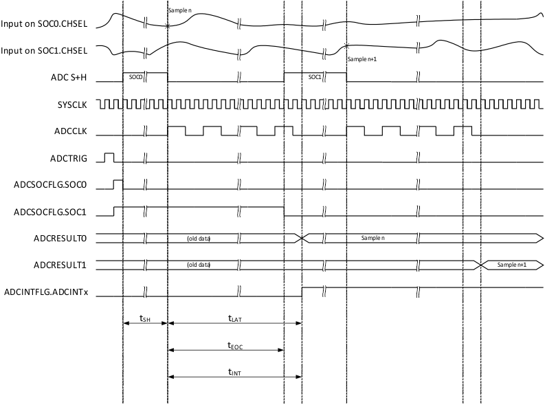 Figure 4-34 ADC Timings for 12-Bit Mode
Table 4-50 ADC Timings in 16-Bit Mode
| ADCCLK PRESCALE | SYSCLK CYCLES | ADCCLK CYCLES | ||||
|---|---|---|---|---|---|---|
| ADCCTL2 [PRESCALE] |
RATIO ADCCLK:SYSCLK |
tEOC | tLAT | tINT(EARLY) | tINT(LATE) | tEOC |
| 0 | 1 | 31 | 32 | 1 | 31 | 31.0 |
| 1 | 1.5 | Invalid | ||||
| 2 | 2 | 60 | 61 | 1 | 60 | 30.0 |
| 3 | 2.5 | 75 | 75 | 1 | 75 | 30.0 |
| 4 | 3 | 90 | 91 | 1 | 90 | 30.0 |
| 5 | 3.5 | 104 | 106 | 1 | 104 | 29.7 |
| 6 | 4 | 119 | 120 | 1 | 119 | 29.8 |
| 7 | 4.5 | 134 | 134 | 1 | 134 | 29.8 |
| 8 | 5 | 149 | 150 | 1 | 149 | 29.8 |
| 9 | 5.5 | 163 | 165 | 1 | 163 | 29.6 |
| 10 | 6 | 178 | 179 | 1 | 178 | 29.7 |
| 11 | 6.5 | 193 | 193 | 1 | 193 | 29.7 |
| 12 | 7 | 208 | 209 | 1 | 208 | 29.7 |
| 13 | 7.5 | 222 | 224 | 1 | 222 | 29.6 |
| 14 | 8 | 237 | 238 | 1 | 237 | 29.6 |
| 15 | 8.5 | 252 | 252 | 1 | 252 | 29.6 |
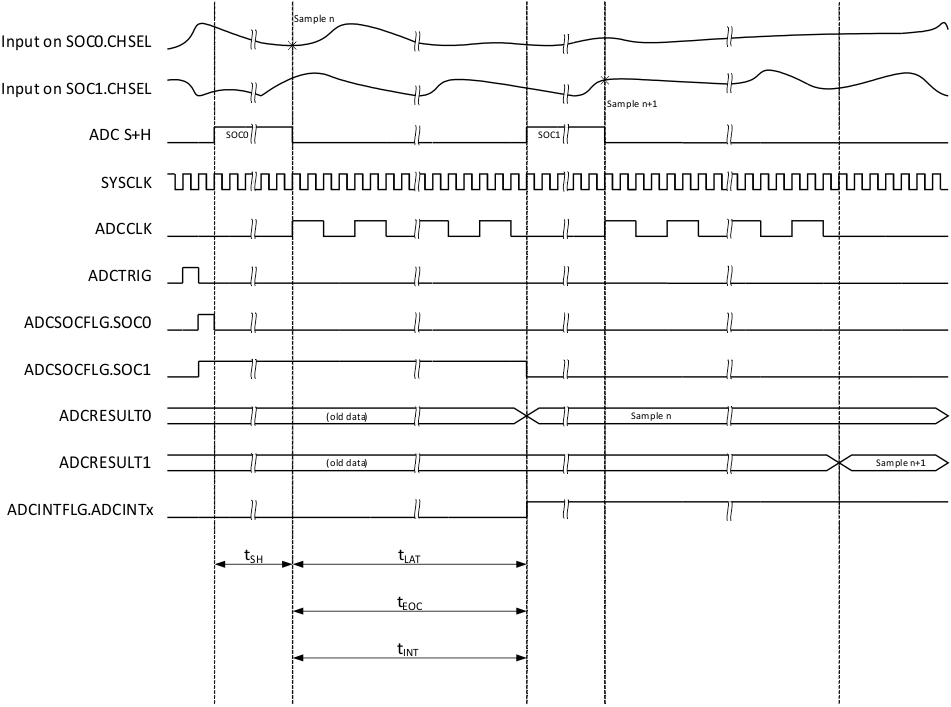 Figure 4-35 ADC Timings for 16-Bit Mode
4.8.1.2 Temperature Sensor Electrical Data and Timing
The temperature sensor can be used to measure the device junction temperature. The temperature sensor is sampled through an internal connection to the ADC and translated into a temperature through TI-provided software. When sampling the temperature sensor, the ADC must meet the acquisition time in Table 4-51.
Table 4-51 Temperature Sensor Electrical Characteristics
over recommended operating conditions (unless otherwise noted)| PARAMETER | MIN | TYP | MAX | UNIT |
|---|---|---|---|---|
| Temperature accuracy | ±15 | °C | ||
| Start-up time (TSNSCTL[ENABLE] to sampling temperature sensor) | 500 | µs | ||
| ADC acquisition time | 700 | ns |
4.8.2 Comparator Subsystem (CMPSS)
Each CMPSS module includes two comparators, two internal voltage reference DACs (CMPSS DACs), two digital glitch filters, and one ramp generator. There are two inputs, CMPINxP and CMPINxN. Each of these inputs will be internally connected to an ADCIN pin. The CMPINxP pin is always connected to the positive input of the CMPSS comparators. CMPINxN can be used instead of the DAC output to drive the negative comparator inputs. There are two comparators, and therefore two outputs from the CMPSS module, which are connected to the input of a digital filter module before being passed on to the Comparator TRIP crossbar and either PWM modules or directly to a GPIO pin. Figure 4-36 shows the CMPSS connectivity on the 337-ball ZWT and 176-pin PTP packages. Figure 4-37 shows CMPSS connectivity on the 100-pin PZP package.
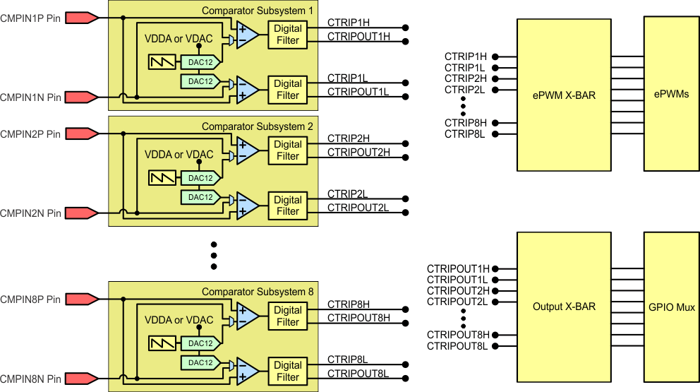 Figure 4-36 CMPSS Connectivity (337-Ball ZWT and 176-Pin PTP)
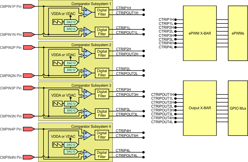 Figure 4-37 CMPSS Connectivity (100-Pin PZP)
4.8.2.1 CMPSS Electrical Data and Timing
Table 4-52 shows the comparator electrical characteristics. Figure 4-38 shows the CMPSS comparator input referred offset. Figure 4-39 shows the CMPSS comparator hysteresis.
Table 4-52 Comparator Electrical Characteristics
over recommended operating conditions (unless otherwise noted)| PARAMETER | TEST CONDITIONS | MIN | TYP | MAX | UNIT |
|---|---|---|---|---|---|
| Power-up time (from COMPCTL[COMPDACE] to comparator ready) | 10 | µs | |||
| Comparator input (CMPINxx) range | 0 | VDDA | V | ||
| Input referred offset error | –20 | 20 | mV | ||
| Hysteresis(1) | 1x | 12 | CMPSS DAC LSB | ||
| 2x | 24 | ||||
| 3x | 36 | ||||
| 4x | 48 | ||||
| Response time (delay from CMPINx input change to output on ePWM X-BAR or Output X-BAR) | Step response | 21 | 60 | ns | |
| Ramp response (1.65 V/µs) | 26 | ||||
| Ramp response (8.25 mV/µs) | 30 |
NOTE
The CMPSS inputs must be kept below VDDA + 0.3 V to ensure proper functional operation. If a CMPSS input exceeds this level, an internal blocking circuit will isolate the internal comparator from the external pin until the external pin voltage returns below VDDA + 0.3 V. During this time, the internal comparator input will be floating and can decay below VDDA within approximately 0.5 µs. After this time, the comparator could begin to output an incorrect result depending on the value of the other comparator input.
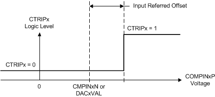 Figure 4-38 CMPSS Comparator Input Referred Offset
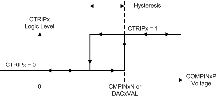 Figure 4-39 CMPSS Comparator Hysteresis
Table 4-53 shows the CMPSS DAC static electrical characteristics. Figure 4-40 shows the CMPSS DAC static offset. Figure 4-41 shows the CMPSS DAC static gain. Figure 4-42 shows the CMPSS DAC static linearity.
Table 4-53 CMPSS DAC Static Electrical Characteristics
over recommended operating conditions (unless otherwise noted)| PARAMETER | TEST CONDITIONS | MIN | TYP | MAX | UNIT |
|---|---|---|---|---|---|
| CMPSS DAC output range | Internal reference | 0 | VDDA | V | |
| External reference | 0 | VDAC | |||
| Static offset error(1) | –25 | 25 | mV | ||
| Static gain error(1) | –2 | 2 | % of FSR | ||
| Static DNL | Endpoint corrected | >–1 | 4 | LSB | |
| Static INL | Endpoint corrected | –16 | 16 | LSB | |
| Settling time | Settling to 1 LSB after full-scale output change | 1 | µs | ||
| Resolution | 12 | bits | |||
| CMPSS DAC output disturbance(2) | Error induced by comparator trip or CMPSS DAC code change within the same CMPSS module | –100 | 100 | LSB | |
| CMPSS DAC disturbance time(2) | 200 | ns | |||
| VDAC reference voltage | When VDAC is reference | 2.4 | 2.5 or 3.0 | VDDA | V |
| VDAC load(3) | When VDAC is reference | 6 | kΩ |
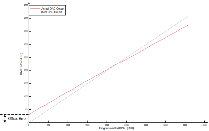 Figure 4-40 CMPSS DAC Static Offset
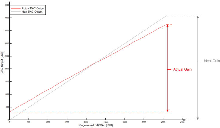 Figure 4-41 CMPSS DAC Static Gain
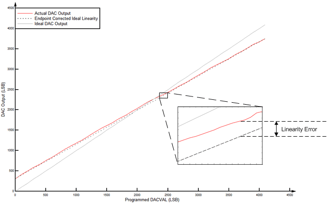 Figure 4-42 CMPSS DAC Static Linearity
4.8.3 Buffered Digital-to-Analog Converter (DAC)
The buffered DAC module consists of an internal reference DAC and an analog output buffer that is capable of driving an external load. An integrated pulldown resistor on the DAC output helps to provide a known pin voltage when the output buffer is disabled. This pulldown resistor cannot be disabled and remains as a passive component on the pin, even for other shared pin mux functions. Software writes to the DAC value register can take effect immediately or can be synchronized with PWMSYNC events.
Each buffered DAC has the following features:
- 12-bit programmable internal DAC
- Selectable reference voltage
- Pulldown resistor on output
- Ability to synchronize with PWMSYNC
The block diagram for the buffered DAC is shown in Figure 4-43.
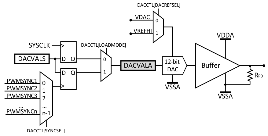 Figure 4-43 DAC Module Block Diagram
4.8.3.1 Buffered DAC Electrical Data and Timing
Table 4-54 shows the buffered DAC electrical characteristics. Figure 4-44 shows the buffered DAC offset. Figure 4-45 shows the buffered DAC gain. Figure 4-46 shows the buffered DAC linearity.
Table 4-54 Buffered DAC Electrical Characteristics
over recommended operating conditions (unless otherwise noted)(1)| PARAMETER | TEST CONDITIONS | MIN | TYP | MAX | UNIT |
|---|---|---|---|---|---|
| Power-up time (DACOUTEN to DAC output valid) | 10 | µs | |||
| Trimmed offset error | Midpoint | –10 | 10 | mV | |
| Gain error(2) | –2.5 | 2.5 | % of FSR | ||
| DNL(3) | Endpoint corrected | > –1 | 1 | LSB | |
| INL | Endpoint corrected | –5 | 5 | LSB | |
| DACOUTx settling time | Settling to 2 LSBs after 0.3V-to-3V transition | 2 | µs | ||
| Resolution | 12 | bits | |||
| Voltage output range(4) | 0.3 | VDDA – 0.3 | V | ||
| Capacitive load | Output drive capability | 100 | pF | ||
| Resistive load | Output drive capability | 5 | kΩ | ||
| RPD | 50 | kΩ | |||
| Reference voltage(5) | VDAC or VREFHI | 2.4 | 2.5 or 3.0 | VDDA | V |
| Reference load(6) | VDAC or VREFHI | 170 | kΩ | ||
| Output noise | Integrated noise from 100 Hz to 100 kHz | 500 | µVrms | ||
| Noise density at 10 kHz | 711 | nVrms/√Hz | |||
| Glitch energy | 1.5 | V-ns | |||
| PSRR(7) | DC up to 1 kHz | 70 | dB | ||
| 100 kHz | 30 | ||||
| SNR | 1020 Hz | 67 | dB | ||
| THD | 1020 Hz | –63 | dB | ||
| SFDR | 1020 Hz, including harmonics and spurs | 66 | dBc | ||
| 1020 Hz, including only spurs | 104 |
NOTE
The VDAC pin must be kept below VDDA + 0.3 V to ensure proper functional operation. If the VDAC pin exceeds this level, a blocking circuit may activate, and the internal value of VDAC may float to 0 V internally, giving improper DAC output.
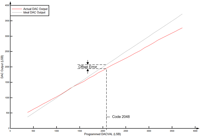 Figure 4-44 Buffered DAC Offset
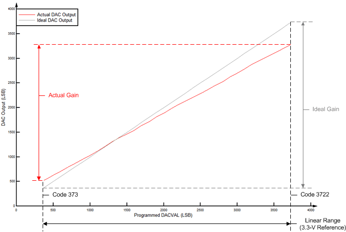 Figure 4-45 Buffered DAC Gain
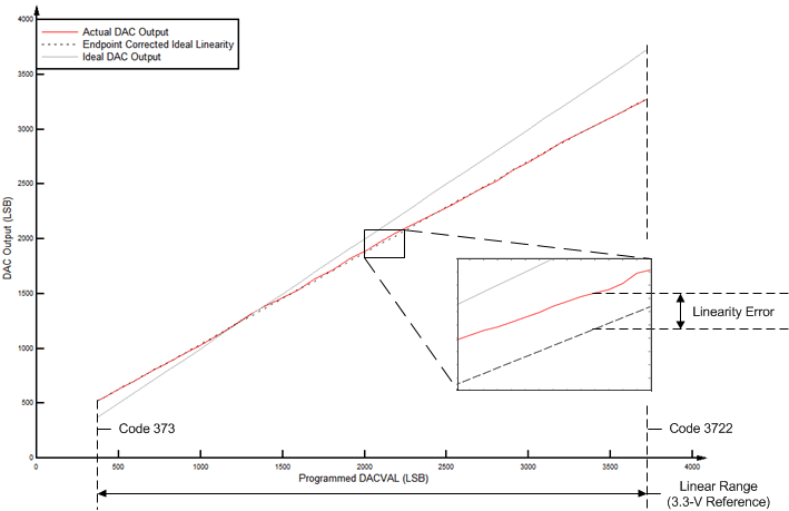 Figure 4-46 Buffered DAC Linearity
4.9 Control Peripherals
4.9.1 Enhanced Capture (eCAP)
The eCAP module can be used in systems where accurate timing of external events is important.
Applications for eCAP include:
- Speed measurements of rotating machinery (for example, toothed sprockets sensed through Hall sensors)
- Elapsed time measurements between position sensor pulses
- Period and duty cycle measurements of pulse train signals
- Decoding current or voltage amplitude derived from duty cycle encoded current/voltage sensors
The eCAP module includes the following features:
- 4-event time-stamp registers (each 32 bits)
- Edge-polarity selection for up to four sequenced time-stamp capture events
- Interrupt on either of the four events
- Single shot capture of up to four event timestamps
- Continuous mode capture of timestamps in a four-deep circular buffer
- Absolute time-stamp capture
- Difference (Delta) mode time-stamp capture
- All of the above resources dedicated to a single input pin
- When not used in capture mode, the eCAP module can be configured as a single-channel PWM output (APWM).
The eCAP inputs connect to any GPIO input through the Input X-BAR. The APWM outputs connect to GPIO pins through the Output X-BAR to OUTPUTx positions in the GPIO mux. See Section 3.4.2 and Section 3.4.3.
Figure 4-47 shows the block diagram of an eCAP module.
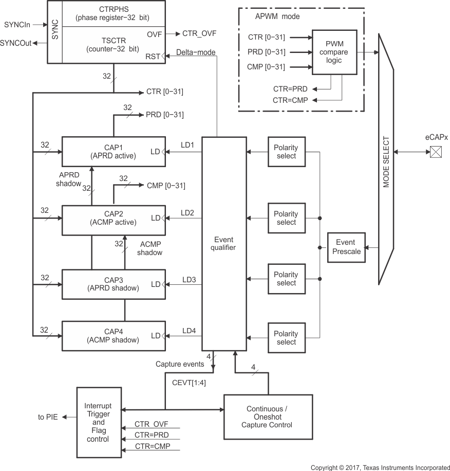 Figure 4-47 eCAP Block Diagram
The eCAP module is clocked by PERx.SYSCLK.
The clock enable bits (ECAP1–ECAP6) in the PCLKCR3 register turn off the eCAP module individually (for low-power operation). Upon reset, ECAP1ENCLK is set to low, indicating that the peripheral clock is off.
4.9.1.1 eCAP Electrical Data and Timing
Table 4-55 shows the eCAP timing requirement and Table 4-56 shows the eCAP switching characteristics.
Table 4-55 eCAP Timing Requirement(1)
| MIN | MAX | UNIT | |||
|---|---|---|---|---|---|
| tw(CAP) | Capture input pulse width | Asynchronous | 2tc(SYSCLK) | cycles | |
| Synchronous | 2tc(SYSCLK) | cycles | |||
| With input qualifier | 1tc(SYSCLK) + tw(IQSW) | cycles | |||
Table 4-56 eCAP Switching Characteristics
over recommended operating conditions (unless otherwise noted)| PARAMETER | MIN | MAX | UNIT | |
|---|---|---|---|---|
| tw(APWM) | Pulse duration, APWMx output high/low | 20 | ns | |
4.9.2 Enhanced Pulse Width Modulator (ePWM)
The ePWM peripheral is a key element in controlling many of the power electronic systems found in both commercial and industrial equipment. The ePWM type-4 module is able to generate complex pulse width waveforms with minimal CPU overhead by building the peripheral up from smaller modules with separate resources that can operate together to form a system. Some of the highlights of the ePWM type-4 module include complex waveform generation, dead-band generation, a flexible synchronization scheme, advanced trip-zone functionality, and global register reload capabilities.
Figure 4-48 shows the signal interconnections with the ePWM. Figure 4-49 shows the ePWM trip input connectivity.
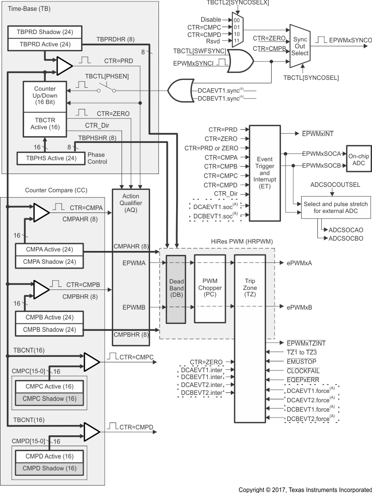
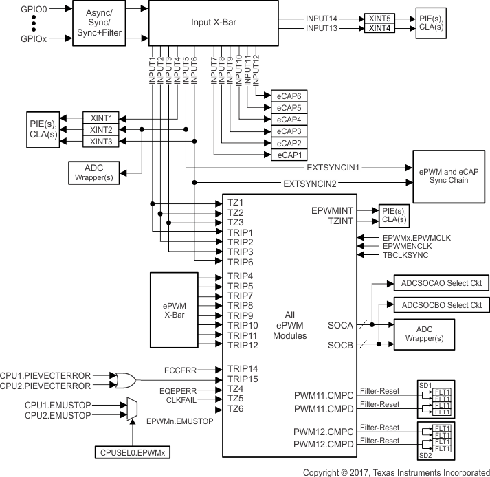 Figure 4-49 ePWM Trip Input Connectivity
4.9.2.1 Control Peripherals Synchronization
The ePWM and eCAP synchronization chain on the device provides flexibility in partitioning the ePWM and eCAP modules between CPU1 and CPU2 and allows localized synchronization within the modules belonging to the same CPU. Like the other peripherals, the partitioning of the ePWM and eCAP modules needs to be done using the CPUSELx registers. Figure 4-50 shows the synchronization chain architecture.
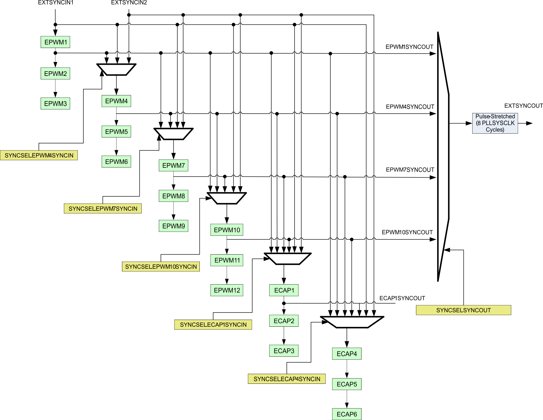 Figure 4-50 Synchronization Chain Architecture
4.9.2.2 ePWM Electrical Data and Timing
Table 4-57 shows the PWM timing requirements and Table 4-58 shows the PWM switching characteristics.
Table 4-57 ePWM Timing Requirements(1)
| MIN | MAX | UNIT | |||
|---|---|---|---|---|---|
| tw(SYNCIN) | Sync input pulse width | Asynchronous | 2tc(EPWMCLK) | cycles | |
| Synchronous | 2tc(EPWMCLK) | cycles | |||
| With input qualifier | 1tc(EPWMCLK) + tw(IQSW) | cycles | |||
Table 4-58 ePWM Switching Characteristics
over recommended operating conditions (unless otherwise noted)| PARAMETER | MIN | MAX | UNIT | |
|---|---|---|---|---|
| tw(PWM) | Pulse duration, PWMx output high/low | 20 | ns | |
| tw(SYNCOUT) | Sync output pulse width | 8tc(SYSCLK) | cycles | |
| td(TZ-PWM) | Delay time, trip input active to PWM forced high Delay time, trip input active to PWM forced low Delay time, trip input active to PWM Hi-Z |
25 | ns | |
4.9.2.2.1 Trip-Zone Input Timing
Table 4-59 shows the trip-zone input timing requirements. Figure 4-51 shows the PWM Hi-Z characteristics.
Table 4-59 Trip-Zone Input Timing Requirements(1)
| MIN | MAX | UNIT | |||
|---|---|---|---|---|---|
| tw(TZ) | Pulse duration, TZx input low | Asynchronous | 1tc(EPWMCLK) | cycles | |
| Synchronous | 2tc(EPWMCLK) | cycles | |||
| With input qualifier | 1tc(EPWMCLK) + tw(IQSW) | cycles | |||

4.9.2.3 External ADC Start-of-Conversion Electrical Data and Timing
Table 4-60 shows the external ADC start-of-conversion switching characteristics. Figure 4-52 shows the ADCSOCAO or ADCSOCBO timing.
Table 4-60 External ADC Start-of-Conversion Switching Characteristics
over recommended operating conditions (unless otherwise noted)| PARAMETER | MIN | MAX | UNIT | |
|---|---|---|---|---|
| tw(ADCSOCL) | Pulse duration, ADCSOCxO low | 32tc(SYSCLK) | cycles | |
 Figure 4-52 ADCSOCAO or ADCSOCBO Timing
4.9.3 Enhanced Quadrature Encoder Pulse (eQEP)
The eQEP module interfaces directly with linear or rotary incremental encoders to obtain position, direction, and speed information from rotating machines used in high-performance motion and position-control systems.
Each eQEP peripheral comprises five major functional blocks:
- Quadrature Capture Unit (QCAP)
- Position Counter/Control Unit (PCCU)
- Quadrature Decoder Unit (QDU)
- Unit Time Base for speed and frequency measurement (UTIME)
- Watchdog timer for detecting stalls (QWDOG)
The eQEP peripherals are clocked by PERx.SYSCLK. Figure 4-53 shows the eQEP block diagram.
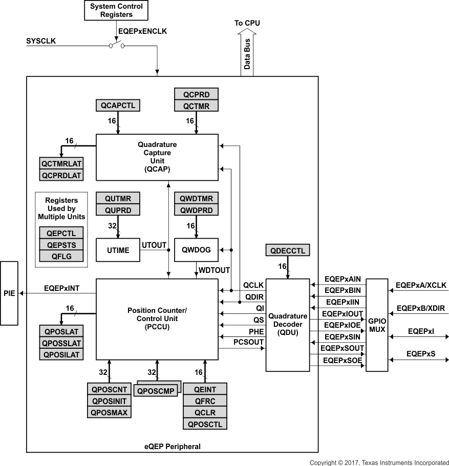 Figure 4-53 eQEP Block Diagram
4.9.3.1 eQEP Electrical Data and Timing
Table 4-61 lists the eQEP timing requirement and Table 4-62 lists the eQEP switching characteristics.
Table 4-61 eQEP Timing Requirements(1)
| MIN | MAX | UNIT | |||
|---|---|---|---|---|---|
| tw(QEPP) | QEP input period | Asynchronous(2)/Synchronous | 2tc(SYSCLK) | cycles | |
| With input qualifier | 2[1tc(SYSCLK) + tw(IQSW)] | cycles | |||
| tw(INDEXH) | QEP Index Input High time | Asynchronous(2)/Synchronous | 2tc(SYSCLK) | cycles | |
| With input qualifier | 2tc(SYSCLK) + tw(IQSW) | cycles | |||
| tw(INDEXL) | QEP Index Input Low time | Asynchronous(2)/Synchronous | 2tc(SYSCLK) | cycles | |
| With input qualifier | 2tc(SYSCLK) + tw(IQSW) | cycles | |||
| tw(STROBH) | QEP Strobe High time | Asynchronous(2)/Synchronous | 2tc(SYSCLK) | cycles | |
| With input qualifier | 2tc(SYSCLK) + tw(IQSW) | cycles | |||
| tw(STROBL) | QEP Strobe Input Low time | Asynchronous(2)/Synchronous | 2tc(SYSCLK) | cycles | |
| With input qualifier | 2tc(SYSCLK) + tw(IQSW) | cycles | |||
Table 4-62 eQEP Switching Characteristics
over recommended operating conditions (unless otherwise noted)| PARAMETER | MIN | MAX | UNIT | |
|---|---|---|---|---|
| td(CNTR)xin | Delay time, external clock to counter increment | 4tc(SYSCLK) | cycles | |
| td(PCS-OUT)QEP | Delay time, QEP input edge to position compare sync output | 6tc(SYSCLK) | cycles | |
4.9.4 High-Resolution Pulse Width Modulator (HRPWM)
The HRPWM combines multiple delay lines in a single module and a simplified calibration system by using a dedicated calibration delay line. For each ePWM module, there are two HR outputs:
- HR Duty and Deadband control on Channel A
- HR Duty and Deadband control on Channel B
The HRPWM module offers PWM resolution (time granularity) that is significantly better than what can be achieved using conventionally derived digital PWM methods. The key points for the HRPWM module are:
- Significantly extends the time resolution capabilities of conventionally derived digital PWM
- This capability can be used in both single edge (duty cycle and phase-shift control) as well as dual edge control for frequency/period modulation.
- Finer time granularity control or edge positioning is controlled through extensions to the Compare A, B, phase, period and deadband registers of the ePWM module.
NOTE
The minimum HRPWMCLK frequency allowed for HRPWM is 60 MHz.
4.9.4.1 HRPWM Electrical Data and Timing
Table 4-63 lists the high-resolution PWM switching characteristics.
Table 4-63 High-Resolution PWM Characteristics
| PARAMETER | MIN | TYP | MAX | UNIT | |
|---|---|---|---|---|---|
| Micro Edge Positioning (MEP) step size(1) | 150 | 310 | ps | ||
Applications that use the HRPWM feature should use MEP Scale Factor Optimizer (SFO) estimation software functions. See the TI software libraries for details of using SFO functions in end applications. SFO functions help to estimate the number of MEP steps per SYSCLK period dynamically while the HRPWM is in operation.
4.9.5 Sigma-Delta Filter Module (SDFM)
The SDFM is a four-channel digital filter designed specifically for current measurement and resolver position decoding in motor control applications. Each channel can receive an independent sigma-delta (ΣΔ) modulated bit stream. The bit streams are processed by four individually programmable digital decimation filters. The filter set includes a fast comparator for immediate digital threshold comparisons for overcurrent and undercurrent monitoring. Figure 4-54 shows a block diagram of the SDFMs.
SDFM features include:
- Eight external pins per SDFM module:
- Four sigma-delta data input pins per SDFM module (SDx_Dy, where x = 1 to 2 and y = 1 to 4)
- Four sigma-delta clock input pins per SDFM module (SDx_Cy, where x = 1 to 2 and y = 1 to 4)
- Four different configurable modulator clock modes:
- Modulator clock rate equals modulator data rate
- Modulator clock rate running at half the modulator data rate
- Modulator data is Manchester encoded. Modulator clock not required.
- Modulator clock rate is double that of modulator data rate
- Four independent configurable comparator units:
- Four different filter type selection (Sinc1/Sinc2/Sincfast/Sinc3) options available
- Ability to detect over-value and under-value conditions
- Comparator Over-Sampling Ratio (COSR) value for comparator programmable from 1 to 32
- Four independent configurable data filter units:
- Four different filter type selection (Sinc1/Sinc2/Sincfast/Sinc3) options available
- Data filter Over-Sampling Ratio (DOSR) value for data filter unit programmable from 1 to 256
- Ability to enable or disable individual filter module
- Ability to synchronize all four independent filters of a SDFM module using the Master Filter Enable (MFE) bit or the PWM signals.
- Filter data can be 16-bit or 32-bit representation
- PWMs can be used to generate modulator clock for sigma-delta modulators
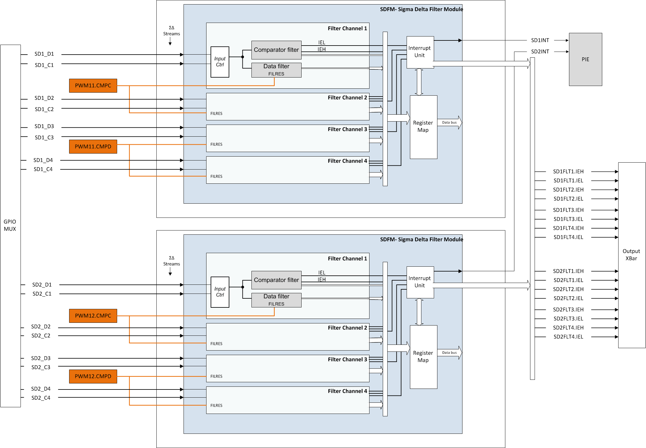 Figure 4-54 SDFM Block Diagram
4.9.5.1 SDFM Electrical Data and Timing
Table 4-64 shows the SDFM timing requirements. Figure 4-55 through Figure 4-58 show the SDFM timing diagrams.
Table 4-64 SDFM Timing Requirements
| MIN | MAX | UNIT | ||
|---|---|---|---|---|
| Mode 0 | ||||
| tc(SDC)M0 | Cycle time, SDx_Cy | 40 | 256 * SYSCLK period | ns |
| tw(SDCH)M0 | Pulse duration, SDx_Cy high | 10 | tc(SDC)M0 – 10 | ns |
| tsu(SDDV-SDCH)M0 | Setup time, SDx_Dy valid before SDx_Cy goes high | 5 | ns | |
| th(SDCH-SDD)M0 | Hold time, SDx_Dy wait after SDx_Cy goes high | 5 | ns | |
| Mode 1 | ||||
| tc(SDC)M1 | Cycle time, SDx_Cy | 80 | 256 * SYSCLK period | ns |
| tw(SDCH)M1 | Pulse duration, SDx_Cy high | 10 | tc(SDC)M1 – 10 | ns |
| tsu(SDDV-SDCL)M1 | Setup time, SDx_Dy valid before SDx_Cy goes low | 5 | ns | |
| tsu(SDDV-SDCH)M1 | Setup time, SDx_Dy valid before SDx_Cy goes high | 5 | ns | |
| th(SDCL-SDD)M1 | Hold time, SDx_Dy wait after SDx_Cy goes low | 5 | ns | |
| th(SDCH-SDD)M1 | Hold time, SDx_Dy wait after SDx_Cy goes high | 5 | ns | |
| Mode 2 | ||||
| tc(SDD)M2 | Cycle time, SDx_Dy | 8 * tc(SYSCLK) | 20 * tc(SYSCLK) | ns |
| tw(SDDH)M2 | Pulse duration, SDx_Dy high | 10 | ns | |
| Mode 3 | ||||
| tc(SDC)M3 | Cycle time, SDx_Cy | 40 | 256 * SYSCLK period | ns |
| tw(SDCH)M3 | Pulse duration, SDx_Cy high | 10 | tc(SDC)M3 – 5 | ns |
| tsu(SDDV-SDCH)M3 | Setup time, SDx_Dy valid before SDx_Cy goes high | 5 | ns | |
| th(SDCH-SDD)M3 | Hold time, SDx_Dy wait after SDx_Cy goes high | 5 | ns | |
 Figure 4-55 SDFM Timing Diagram – Mode 0
 Figure 4-56 SDFM Timing Diagram – Mode 1
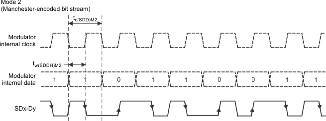 Figure 4-57 SDFM Timing Diagram – Mode 2
 Figure 4-58 SDFM Timing Diagram – Mode 3
4.10 Communications Peripherals
4.10.1 Controller Area Network (CAN)
NOTE
The CAN module uses the IP known as D_CAN. This document uses the names CAN and D_CAN interchangeably to reference this peripheral.
The CAN module implements the following features:
- Complies with ISO 11898-1 (Bosch® CAN protocol specification 2.0 A and B)
- Bit rates up to 1 Mbps
- Multiple clock sources
- 32 message objects, each with the following properties:
- Configurable as receive or transmit
- Configurable with standard or extended identifier
- Programmable receive and identifier masks for each object
- Supports data and remote frames
- Holds 0 to 8 bytes of data
- Parity-checked configuration and data RAM
- Individual identifier mask for each message object
- Programmable FIFO mode for receive message objects
- Programmable loop-back modes for self-test operation
- Suspend mode for debug support
- Software module reset
- Automatic bus on after Bus-Off state by a programmable 32-bit timer
- Message RAM parity check mechanism
- Two interrupt lines
- Global power down and wakeup support
NOTE
For a CANx Bit-CLK of 200 MHz, the smallest bit rate possible is 7.8125 kbps.
NOTE
The accuracy of the on-chip zero-pin oscillator is in Table 4-18, Internal Oscillator Electrical Characteristics. Depending on parameters such as the CAN bit timing settings, bit rate, bus length, and propagation delay, the accuracy of this oscillator may not meet the requirements of the CAN protocol. In this situation, an external clock source must be used.
4.10.2 Inter-Integrated Circuit (I2C)
The I2C module has the following features:
- Compliance with the Philips Semiconductors I2C-bus specification (version 2.1):
- Support for 1-bit to 8-bit format transfers
- 7-bit and 10-bit addressing modes
- General call
- START byte mode
- Support for multiple master-transmitters and slave-receivers
- Support for multiple slave-transmitters and master-receivers
- Combined master transmit/receive and receive/transmit mode
- Data transfer rate of from 10 kbps up to 400 kbps (I2C Fast-mode rate)
- One 16-byte receive FIFO and one 16-byte transmit FIFO
- One interrupt that can be used by the CPU. This interrupt can be generated as a result of one of the following conditions:
- Transmit-data ready
- Receive-data ready
- Register-access ready
- No-acknowledgment received
- Arbitration lost
- Stop condition detected
- Addressed as slave
- An additional interrupt that can be used by the CPU when in FIFO mode
- Module enable/disable capability
- Free data format mode
Figure 4-59 shows how the I2C peripheral module interfaces within the device.
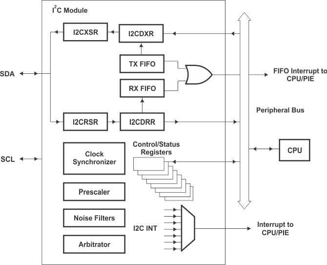 Figure 4-59 I2C Peripheral Module Interfaces
4.10.2.1 I2C Electrical Data and Timing
Table 4-65 shows the I2C timing requirements. Table 4-66 shows the I2C switching characteristics.
Table 4-65 I2C Timing Requirements
| MIN | MAX | UNIT | |||
|---|---|---|---|---|---|
| th(SDA-SCL)START | Hold time, START condition, SCL fall delay after SDA fall | 0.6 | µs | ||
| tsu(SCL-SDA)START | Setup time, Repeated START, SCL rise before SDA fall delay | 0.6 | µs | ||
| th(SCL-DAT) | Hold time, data after SCL fall | 0 | µs | ||
| tsu(DAT-SCL) | Setup time, data before SCL rise | 100 | ns | ||
| tr(SDA) | Rise time, SDA | Input tolerance | 20 | 300 | ns |
| tr(SCL) | Rise time, SCL | Input tolerance | 20 | 300 | ns |
| tf(SDA) | Fall time, SDA | Input tolerance | 11.4 | 300 | ns |
| tf(SCL) | Fall time, SCL | Input tolerance | 11.4 | 300 | ns |
| tsu(SCL-SDA)STOP | Setup time, STOP condition, SCL rise before SDA rise delay | 0.6 | µs | ||
Table 4-66 I2C Switching Characteristics
over recommended operating conditions (unless otherwise noted)| PARAMETER | TEST CONDITIONS | MIN | MAX | UNIT | |
|---|---|---|---|---|---|
| fSCL | SCL clock frequency | 0 | 400 | kHz | |
| tw(SCLL) | Pulse duration, SCL clock low | 1.3 | µs | ||
| tw(SCLH) | Pulse duration, SCL clock high | 0.6 | µs | ||
| tw(SP) | Pulse duration of spikes that will be suppressed by the input filter | 0 | 50 | ns | |
| tBUF | Bus free time between STOP and START conditions | 1.3 | µs | ||
| tv(SCL-DAT) | Valid time, data after SCL fall | 0.9 | µs | ||
| tv(SCL-ACK) | Valid time, Acknowledge after SCL fall | 0.9 | µs | ||
| VIL | Valid low-level input voltage | –0.3 | 0.3 * VDDIO | V | |
| VIH | Valid high-level input voltage | 0.7 * VDDIO | VDDIO + 0.3 | V | |
| VOL | Low-level output voltage | Sinking 3 mA | 0 | 0.4 | V |
| II | Input current on pins | 0.1 Vbus < Vi < 0.9 Vbus | –10 | 10 | µA |
NOTE
To meet all of the I2C protocol timing specifications, the I2C module clock must be configured between 7 MHz to 12 MHz.
4.10.3 Multichannel Buffered Serial Port (McBSP)
The McBSP module has the following features:
- Compatible with McBSP in TMS320C28x and TMS320F28x DSP devices
- Full-duplex communication
- Double-buffered data registers that allow a continuous data stream
- Independent framing and clocking for receive and transmit
- External shift clock generation or an internal programmable frequency shift clock
- 8-bit data transfer mode can be configured to transmit with LSB or MSB first
- Programmable polarity for both frame synchronization and data clocks
- Highly programmable internal clock and frame generation
- Direct interface to industry-standard CODECs, Analog Interface Chips (AICs), and other serially connected A/D and D/A devices
- Supports AC97, I2S, and SPI protocols
- McBSP clock rate,

where CLKSRG source could be LSPCLK, CLKX, or CLKR.
Figure 4-60 shows the block diagram of the McBSP module.
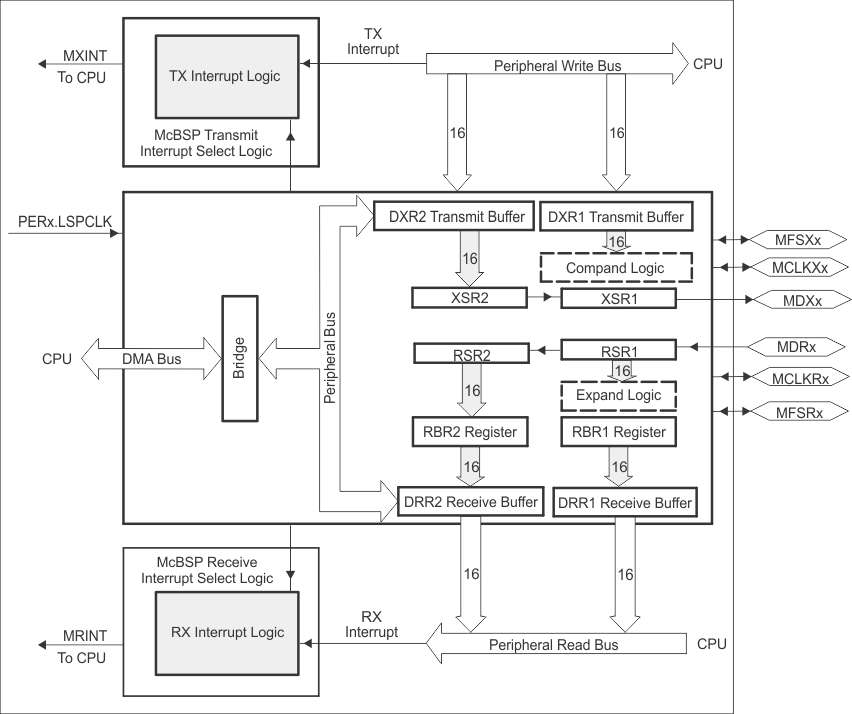 Figure 4-60 McBSP Block Diagram
4.10.3.1 McBSP Electrical Data and Timing
4.10.3.1.1 McBSP Transmit and Receive Timing
Table 4-67 shows the McBSP timing requirements. Table 4-68 shows the McBSP switching characteristics. Figure 4-61 and Figure 4-62 show the McBSP timing diagrams.
Table 4-67 McBSP Timing Requirements(1) (2)
| NO. | MIN | MAX | UNIT | |||
|---|---|---|---|---|---|---|
| McBSP module clock (CLKG, CLKX, CLKR) range | 1 | kHz | ||||
| 25 | MHz | |||||
| McBSP module cycle time (CLKG, CLKX, CLKR) range | 40 | ns | ||||
| 1 | ms | |||||
| M11 | tc(CKRX) | Cycle time, CLKR/X | CLKR/X ext | 2P | ns | |
| M12 | tw(CKRX) | Pulse duration, CLKR/X high or CLKR/X low | CLKR/X ext | P – 7 | ns | |
| M13 | tr(CKRX) | Rise time, CLKR/X | CLKR/X ext | 7 | ns | |
| M14 | tf(CKRX) | Fall time, CLKR/X | CLKR/X ext | 7 | ns | |
| M15 | tsu(FRH-CKRL) | Setup time, external FSR high before CLKR low | CLKR int | 18 | ns | |
| CLKR ext | 2 | |||||
| M16 | th(CKRL-FRH) | Hold time, external FSR high after CLKR low | CLKR int | 0 | ns | |
| CLKR ext | 6 | |||||
| M17 | tsu(DRV-CKRL) | Setup time, DR valid before CLKR low | CLKR int | 18 | ns | |
| CLKR ext | 5 | |||||
| M18 | th(CKRL-DRV) | Hold time, DR valid after CLKR low | CLKR int | 0 | ns | |
| CLKR ext | 3 | |||||
| M19 | tsu(FXH-CKXL) | Setup time, external FSX high before CLKX low | CLKX int | 18 | ns | |
| CLKX ext | 2 | |||||
| M20 | th(CKXL-FXH) | Hold time, external FSX high after CLKX low | CLKX int | 0 | ns | |
| CLKX ext | 6 | |||||
Table 4-68 McBSP Switching Characteristics(1) (2)
over recommended operating conditions (unless otherwise noted)| NO. | PARAMETER | MIN | MAX | UNIT | |||
|---|---|---|---|---|---|---|---|
| M1 | tc(CKRX) | Cycle time, CLKR/X | CLKR/X int | 2P | ns | ||
| M2 | tw(CKRXH) | Pulse duration, CLKR/X high | CLKR/X int | D – 5 (3) | D + 5 (3) | ns | |
| M3 | tw(CKRXL) | Pulse duration, CLKR/X low | CLKR/X int | C – 5 (3) | C + 5 (3) | ns | |
| M4 | td(CKRH-FRV) | Delay time, CLKR high to internal FSR valid | CLKR int | 0 | 4 | ns | |
| CLKR ext | 3 | 27 | |||||
| M5 | td(CKXH-FXV) | Delay time, CLKX high to internal FSX valid | CLKX int | 0 | 4 | ns | |
| CLKX ext | 3 | 27 | |||||
| M6 | tdis(CKXH-DXHZ) | Disable time, CLKX high to DX high impedance following last data bit | CLKX int | 8 | ns | ||
| CLKX ext | 14 | ||||||
| M7 | td(CKXH-DXV) | Delay time, CLKX high to DX valid. | CLKX int | 9 | ns | ||
| This applies to all bits except the first bit transmitted. | CLKX ext | 28 | |||||
| Delay time, CLKX high to DX valid | DXENA = 0 | CLKX int | 8 | ||||
| CLKX ext | 14 | ||||||
| Only applies to first bit transmitted when in Data Delay 1 or 2 (XDATDLY=01b or 10b) modes | DXENA = 1 | CLKX int | P + 8 | ||||
| CLKX ext | P + 14 | ||||||
| M8 | ten(CKXH-DX) | Enable time, CLKX high to DX driven | DXENA = 0 | CLKX int | 0 | ns | |
| CLKX ext | 6 | ||||||
| Only applies to first bit transmitted when in Data Delay 1 or 2 (XDATDLY=01b or 10b) modes | DXENA = 1 | CLKX int | P | ||||
| CLKX ext | P + 6 | ||||||
| M9 | td(FXH-DXV) | Delay time, FSX high to DX valid | DXENA = 0 | FSX int | 8 | ns | |
| FSX ext | 14 | ||||||
| Only applies to first bit transmitted when in Data Delay 0 (XDATDLY=00b) mode. | DXENA = 1 | FSX int | P + 8 | ||||
| FSX ext | P + 14 | ||||||
| M10 | ten(FXH-DX) | Enable time, FSX high to DX driven | DXENA = 0 | FSX int | 0 | ns | |
| FSX ext | 6 | ||||||
| Only applies to first bit transmitted when in Data Delay 0 (XDATDLY=00b) mode | DXENA = 1 | FSX int | P | ||||
| FSX ext | P + 6 | ||||||
D = CLKRX high pulse width = P
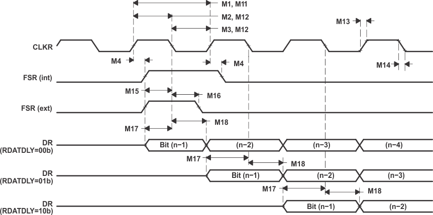 Figure 4-61 McBSP Receive Timing
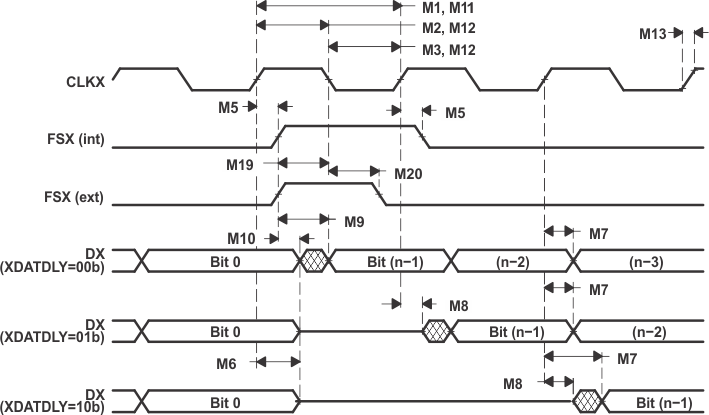 Figure 4-62 McBSP Transmit Timing
4.10.3.1.2 McBSP as SPI Master or Slave Timing
For CLKSTP = 10b and CLKXP = 0, Table 4-69 shows the timing requirements, Table 4-70 shows the switching characteristics, and Figure 4-63 shows the timing diagram.
Table 4-69 McBSP as SPI Master or Slave Timing Requirements (CLKSTP = 10b, CLKXP = 0)(1)
| NO. | MASTER | SLAVE | UNIT | ||||
|---|---|---|---|---|---|---|---|
| MIN | MAX | MIN | MAX | ||||
| M30 | tsu(DRV-CKXL) | Setup time, DR valid before CLKX low | 30 | 8P – 10 | ns | ||
| M31 | th(CKXL-DRV) | Hold time, DR valid after CLKX low | 1 | 8P – 10 | ns | ||
| M32 | tsu(BFXL-CKXH) | Setup time, FSX low before CLKX high | 8P + 10 | ns | |||
| M33 | tc(CKX) | Cycle time, CLKX | 2P(2) | 16P | ns | ||
Table 4-70 McBSP as SPI Master or Slave Switching Characteristics (CLKSTP = 10b, CLKXP = 0)
| NO. | PARAMETER | MASTER | SLAVE | UNIT | |||
|---|---|---|---|---|---|---|---|
| MIN | MAX | MIN | MAX | ||||
| M24 | th(CKXL-FXL) | Hold time, FSX low after CLKX low | 2P(1) | ns | |||
| M25 | td(FXL-CKXH) | Delay time, FSX low to CLKX high | P | ns | |||
| M28 | tdis(FXH-DXHZ) | Disable time, DX high impedance following last data bit from FSX high | 6 | 6P + 6 | ns | ||
| M29 | td(FXL-DXV) | Delay time, FSX low to DX valid | 6 | 4P + 6 | ns | ||
 Figure 4-63 McBSP Timing as SPI Master or Slave: CLKSTP = 10b, CLKXP = 0
For CLKSTP = 11b and CLKXP = 0, Table 4-71 shows the timing requirements, Table 4-72 shows the switching characteristics, and Figure 4-64 shows the timing diagram.
Table 4-71 McBSP as SPI Master or Slave Timing Requirements (CLKSTP = 11b, CLKXP = 0)(1)
| NO. | MASTER | SLAVE | UNIT | ||||
|---|---|---|---|---|---|---|---|
| MIN | MAX | MIN | MAX | ||||
| M39 | tsu(DRV-CKXH) | Setup time, DR valid before CLKX high | 30 | 8P – 10 | ns | ||
| M40 | th(CKXH-DRV) | Hold time, DR valid after CLKX high | 1 | 8P – 10 | ns | ||
| M41 | tsu(FXL-CKXH) | Setup time, FSX low before CLKX high | 16P + 10 | ns | |||
| M42 | tc(CKX) | Cycle time, CLKX | 2P(2) | 16P | ns | ||
Table 4-72 McBSP as SPI Master or Slave Switching Characteristics (CLKSTP = 11b, CLKXP = 0)
| NO. | PARAMETER | MASTER | SLAVE | UNIT | |||
|---|---|---|---|---|---|---|---|
| MIN | MAX | MIN | MAX | ||||
| M34 | th(CKXL-FXL) | Hold time, FSX low after CLKX low | P | ns | |||
| M35 | td(FXL-CKXH) | Delay time, FSX low to CLKX high | 2P(1) | ns | |||
| M37 | tdis(CKXL-DXHZ) | Disable time, DX high impedance following last data bit from CLKX low | P + 6 | 7P + 6 | ns | ||
| M38 | td(FXL-DXV) | Delay time, FSX low to DX valid | 6 | 4P + 6 | ns | ||
 Figure 4-64 McBSP Timing as SPI Master or Slave: CLKSTP = 11b, CLKXP = 0
For CLKSTP = 10b and CLKXP = 1, Table 4-73 shows the timing requirements, Table 4-74 shows the switching characteristics, and Figure 4-65 shows the timing diagram.
Table 4-73 McBSP as SPI Master or Slave Timing Requirements (CLKSTP = 10b, CLKXP = 1)(1)
| NO. | MASTER | SLAVE | UNIT | ||||
|---|---|---|---|---|---|---|---|
| MIN | MAX | MIN | MAX | ||||
| M49 | tsu(DRV-CKXH) | Setup time, DR valid before CLKX high | 30 | 8P – 10 | ns | ||
| M50 | th(CKXH-DRV) | Hold time, DR valid after CLKX high | 1 | 8P – 10 | ns | ||
| M51 | tsu(FXL-CKXL) | Setup time, FSX low before CLKX low | 8P + 10 | ns | |||
| M52 | tc(CKX) | Cycle time, CLKX | 2P(2) | 16P | ns | ||
Table 4-74 McBSP as SPI Master or Slave Switching Characteristics (CLKSTP = 10b, CLKXP = 1)
| NO. | PARAMETER | MASTER | SLAVE | UNIT | |||
|---|---|---|---|---|---|---|---|
| MIN | MAX | MIN | MAX | ||||
| M43 | th(CKXH-FXL) | Hold time, FSX low after CLKX high | 2P(1) | ns | |||
| M44 | td(FXL-CKXL) | Delay time, FSX low to CLKX low | P | ns | |||
| M47 | tdis(FXH-DXHZ) | Disable time, DX high impedance following last data bit from FSX high | 6 | 6P + 6 | ns | ||
| M48 | td(FXL-DXV) | Delay time, FSX low to DX valid | 6 | 4P + 6 | ns | ||
 Figure 4-65 McBSP Timing as SPI Master or Slave: CLKSTP = 10b, CLKXP = 1
For CLKSTP = 11b and CLKXP = 1, Table 4-75 shows the timing requirements, Table 4-76 shows the switching characteristics, and Figure 4-66 shows the timing diagram.
Table 4-75 McBSP as SPI Master or Slave Timing Requirements (CLKSTP = 11b, CLKXP = 1)(1)
| NO. | MASTER | SLAVE | UNIT | ||||
|---|---|---|---|---|---|---|---|
| MIN | MAX | MIN | MAX | ||||
| M58 | tsu(DRV-CKXL) | Setup time, DR valid before CLKX low | 30 | 8P – 10 | ns | ||
| M59 | th(CKXL-DRV) | Hold time, DR valid after CLKX low | 1 | 8P – 10 | ns | ||
| M60 | tsu(FXL-CKXL) | Setup time, FSX low before CLKX low | 16P + 10 | ns | |||
| M61 | tc(CKX) | Cycle time, CLKX | 2P(2) | 16P | ns | ||
Table 4-76 McBSP as SPI Master or Slave Switching Characteristics (CLKSTP = 11b, CLKXP = 1)(1)
| NO. | PARAMETER | MASTER(2) | SLAVE | UNIT | |||
|---|---|---|---|---|---|---|---|
| MIN | MAX | MIN | MAX | ||||
| M53 | th(CKXH-FXL) | Hold time, FSX low after CLKX high | P | ns | |||
| M54 | td(FXL-CKXL) | Delay time, FSX low to CLKX low | 2P(1) | ns | |||
| M55 | td(CLKXH-DXV) | Delay time, CLKX high to DX valid | –2 | 0 | 3P + 6 | 5P + 20 | ns |
| M56 | tdis(CKXH-DXHZ) | Disable time, DX high impedance following last data bit from CLKX high | P + 6 | 7P + 6 | ns | ||
| M57 | td(FXL-DXV) | Delay time, FSX low to DX valid | 6 | 4P + 6 | ns | ||
D = CLKX high pulse width = P
 Figure 4-66 McBSP Timing as SPI Master or Slave: CLKSTP = 11b, CLKXP = 1
4.10.4 Serial Communications Interface (SCI)
The SCI is a 2-wire asynchronous serial port, commonly known as a UART. The SCI module supports digital communications between the CPU and other asynchronous peripherals that use the standard non-return-to-zero (NRZ) format
The SCI receiver and transmitter each have a 16-level-deep FIFO for reducing servicing overhead, and each has its own separate enable and interrupt bits. Both can be operated independently for half-duplex communication, or simultaneously for full-duplex communication. To specify data integrity, the SCI checks received data for break detection, parity, overrun, and framing errors. The bit rate is programmable to different speeds through a 16-bit baud-select register. Figure 4-67 shows the SCI block diagram.
Features of the SCI module include:
- Two external pins:
- SCITXD: SCI transmit-output pin
- SCIRXD: SCI receive-input pin
- Baud rate programmable to 64K different rates
NOTE: Both pins can be used as GPIO if not used for SCI.
- Data-word format
- One start bit
- Data-word length programmable from 1 to 8 bits
- Optional even/odd/no parity bit
- 1 or 2 stop bits
- Four error-detection flags: parity, overrun, framing, and break detection
- Two wakeup multiprocessor modes: idle-line and address bit
- Half- or full-duplex operation
- Double-buffered receive and transmit functions
- Transmitter and receiver operations can be accomplished through interrupt-driven or polled algorithms with status flags.
- Transmitter: TXRDY flag (transmitter-buffer register is ready to receive another character) and TX EMPTY flag (transmitter-shift register is empty)
- Receiver: RXRDY flag (receiver-buffer register is ready to receive another character), BRKDT flag (break condition occurred), and RX ERROR flag (monitoring four interrupt conditions)
- Separate enable bits for transmitter and receiver interrupts (except BRKDT)
- NRZ format
- Auto baud-detect hardware logic
- 16-level transmit and receive FIFO
NOTE
All registers in this module are 8-bit registers. When a register is accessed, the register data is in the lower byte (bits 7–0), and the upper byte (bits 15–8) is read as zeros. Writing to the upper byte has no effect.
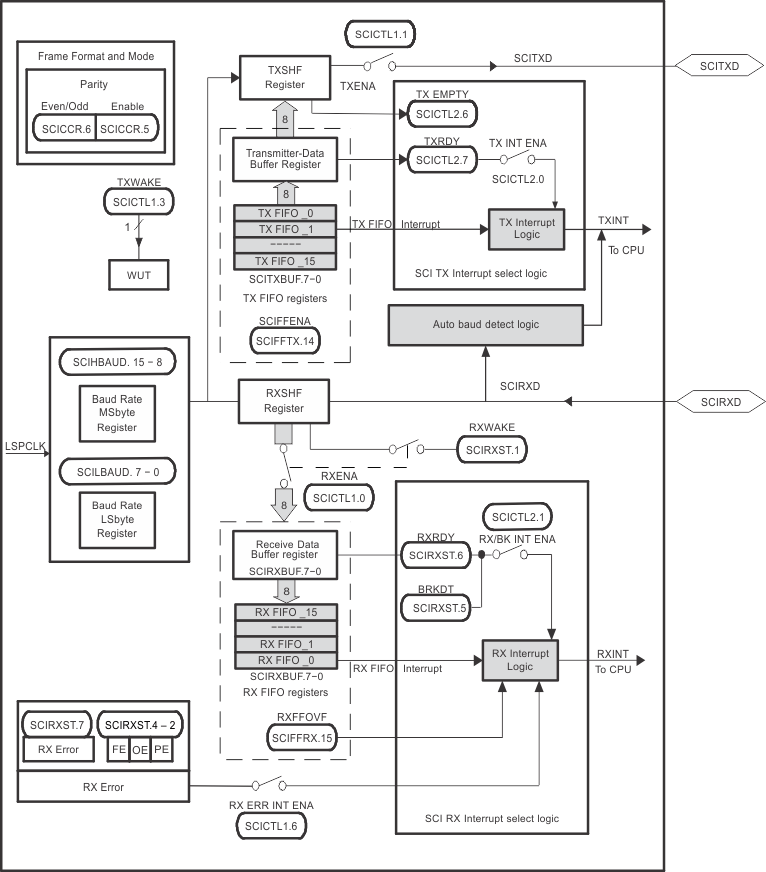 Figure 4-67 SCI Block Diagram
The major elements used in full-duplex operation include:
- A transmitter (TX) and its major registers:
- SCITXBUF register – Transmitter Data Buffer register. Contains data (loaded by the CPU) to be transmitted
- TXSHF register – Transmitter Shift register. Accepts data from the SCITXBUF register and shifts data onto the SCITXD pin, 1 bit at a time
- A receiver (RX) and its major registers:
- RXSHF register – Receiver Shift register. Shifts data in from the SCIRXD pin, 1 bit at a time
- SCIRXBUF register – Receiver Data Buffer register. Contains data to be read by the CPU. Data from a remote processor is loaded into the RXSHF register and then into the SCIRXBUF and SCIRXEMU registers
- A programmable baud generator
- Data-memory-mapped control and status registers enable the CPU to access the I2C module registers and FIFOs.
The SCI receiver and transmitter operate independently.
4.10.5 Serial Peripheral Interface (SPI)
The SPI is a high-speed synchronous serial input/output (I/O) port that allows a serial bit stream of programmed length (1 to 16 bits) to be shifted into and out of the device at a programmed bit-transfer rate. The SPI is normally used for communications between the microcontroller and external peripherals or another controller. Typical applications include external I/O or peripheral expansion through devices such as shift registers, display drivers, and ADCs. Multidevice communications are supported by the master/slave operation of the SPI. The port supports 16-level receive and transmit FIFOs for reducing CPU servicing overhead.
The SPI module features include:
- SPISOMI: SPI slave-output/master-input pin
- SPISIMO: SPI slave-input/master-output pin
- SPISTE: SPI slave transmit-enable pin
- SPICLK: SPI serial-clock pin
- Two operational modes: master and slave
- Baud rate: 125 different programmable rates
- Data word length: 1 to 16 data bits
- Four clocking schemes (controlled by clock polarity and clock phase bits) include:
- Falling edge without phase delay: SPICLK active-high. SPI transmits data on the falling edge of the SPICLK signal and receives data on the rising edge of the SPICLK signal.
- Falling edge with phase delay: SPICLK active-high. SPI transmits data one half-cycle ahead of the falling edge of the SPICLK signal and receives data on the falling edge of the SPICLK signal.
- Rising edge without phase delay: SPICLK inactive-low. SPI transmits data on the rising edge of the SPICLK signal and receives data on the falling edge of the SPICLK signal.
- Rising edge with phase delay: SPICLK inactive-low. SPI transmits data one half-cycle ahead of the rising edge of the SPICLK signal and receives data on the rising edge of the SPICLK signal.
- Simultaneous receive-and-transmit operation (transmit function can be disabled in software)
- Transmitter and receiver operations are accomplished through either interrupt-driven or polled algorithms.
- 16-level transmit and receive FIFO
- Delayed transmit control
- 3-wire SPI mode
- SPISTE inversion for digital audio interface receive mode on devices with two SPI modules
- DMA support
- High-speed mode for up to 50-MHz full-duplex communication
The SPI operates in master or slave mode. The master initiates data transfer by sending the SPICLK signal. For both the slave and the master, data is shifted out of the shift registers on one edge of the SPICLK and latched into the shift register on the opposite SPICLK clock edge. If the CLOCK PHASE bit (SPICTL.3) is high, data is transmitted and received a half-cycle before the SPICLK transition. As a result, both controllers send and receive data simultaneously. The application software determines whether the data is meaningful or dummy data. There are three possible methods for data transmission:
- Master sends data; slave sends dummy data
- Master sends data; slave sends data
- Master sends dummy data; slave sends data
The master can initiate a data transfer at any time because it controls the SPICLK signal. The software, however, determines how the master detects when the slave is ready to broadcast data.
Figure 4-68 shows the SPI CPU Interface.
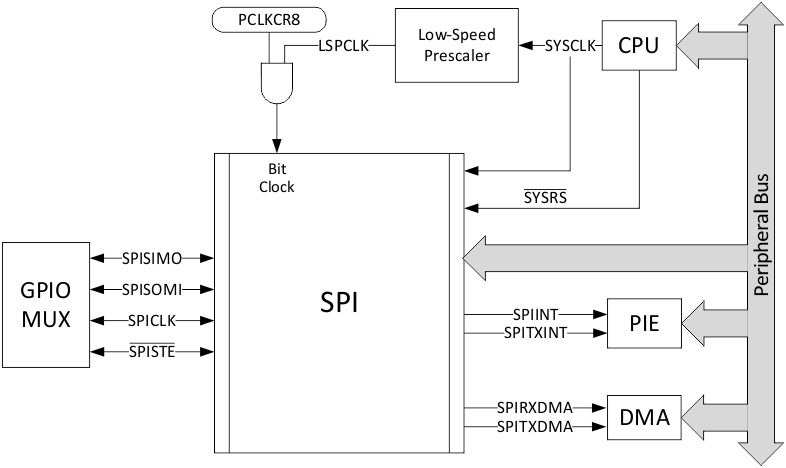 Figure 4-68 SPI CPU Interface
4.10.5.1 SPI Electrical Data and Timing
The following sections contain the SPI External Timings in Non-High-Speed Mode:
| Section 4.10.5.1.1 | Non-High-Speed Master Mode Timings |
| Section 4.10.5.1.2 | Non-High-Speed Slave Mode Timings |
The following sections contain the SPI External Timings in High-Speed Mode:
| Section 4.10.5.1.3 | High-Speed Master Mode Timings |
| Section 4.10.5.1.4 | High-Speed Slave Mode Timings |
NOTE
All timing parameters for SPI High-Speed Mode assume a load capacitance of 5 pF on SPICLK, SPISIMO, and SPISOMI.
For more information about the SPI in High-Speed mode, see the Serial Peripheral Interface (SPI) chapter of the TMS320F2837xD Dual-Core Delfino Microcontrollers Technical Reference Manual.
To use the SPI in High-Speed mode, the application must use the high-speed enabled GPIOs (see Section 3.4.5).
4.10.5.1.1 Non-High-Speed Master Mode Timings
Table 4-77 lists the SPI master mode switching characteristics where the clock phase = 0. Figure 4-69 shows the SPI master mode external timing where the clock phase = 0.
Table 4-78 lists the SPI master mode switching characteristics where the clock phase = 1. Figure 4-70 shows the SPI master mode external timing where the clock phase = 1.
Table 4-79 lists the SPI master mode timing requirements.
Table 4-77 SPI Master Mode Switching Characteristics (Clock Phase = 0)
over recommended operating conditions (unless otherwise noted)| NO. | PARAMETER | (BRR + 1) CONDITION(1) | MIN | MAX | UNIT | |
|---|---|---|---|---|---|---|
| 1 | tc(SPC)M | Cycle time, SPICLK | Even | 4tc(LSPCLK) | 128tc(LSPCLK) | ns |
| Odd | 5tc(LSPCLK) | 127tc(LSPCLK) | ||||
| 2 | tw(SPC1)M | Pulse duration, SPICLK, first pulse | Even | 0.5tc(SPC)M – 3 | 0.5tc(SPC)M + 3 | ns |
| Odd | 0.5tc(SPC)M + 0.5tc(LSPCLK) – 3 |
0.5tc(SPC)M + 0.5tc(LSPCLK) + 3 |
||||
| 3 | tw(SPC2)M | Pulse duration, SPICLK, second pulse | Even | 0.5tc(SPC)M – 3 | 0.5tc(SPC)M + 3 | ns |
| Odd | 0.5tc(SPC)M – 0.5tc(LSPCLK) – 3 |
0.5tc(SPC)M – 0.5tc(LSPCLK) + 3 |
||||
| 4 | td(SIMO)M | Delay time, SPICLK to SPISIMO valid | Even, Odd | 3 | ns | |
| 5 | tv(SIMO)M | Valid time, SPISIMO valid after SPICLK | Even | 0.5tc(SPC)M – 3 | ns | |
| Odd | 0.5tc(SPC)M – 0.5tc(LSPCLK) – 3 |
|||||
| 23 | td(SPC)M | Delay time, SPISTE active to SPICLK | Even | tc(SPC)M – 3 | ns | |
| Odd | 0.5tc(SPC)M – 0.5tc(LSPCLK) – 3 |
|||||
| 24 | td(STE)M | Delay time, SPICLK to SPISTE inactive | Even | 0.5tc(SPC)M – 3 | ns | |
| Odd | 0.5tc(SPC)M – 0.5tc(LSPCLK) – 3 |
|||||
Table 4-78 SPI Master Mode Switching Characteristics (Clock Phase = 1)
over recommended operating conditions (unless otherwise noted)| NO. | PARAMETER | (BRR + 1) CONDITION(1) | MIN | MAX | UNIT | |
|---|---|---|---|---|---|---|
| 1 | tc(SPC)M | Cycle time, SPICLK | Even | 4tc(LSPCLK) | 128tc(LSPCLK) | ns |
| Odd | 5tc(LSPCLK) | 127tc(LSPCLK) | ||||
| 2 | tw(SPC1)M | Pulse duration, SPICLK, first pulse | Even | 0.5tc(SPC)M – 3 | 0.5tc(SPC)M + 3 | ns |
| Odd | 0.5tc(SPC)M – 0.5tc(LSPCLK) – 3 |
0.5tc(SPC)M – 0.5tc(LSPCLK) + 3 |
||||
| 3 | tw(SPC2)M | Pulse duration, SPICLK, second pulse | Even | 0.5tc(SPC)M – 3 | 0.5tc(SPC)M + 3 | ns |
| Odd | 0.5tc(SPC)M + 0.5tc(LSPCLK) – 3 |
0.5tc(SPC)M + 0.5tc(LSPCLK) + 3 |
||||
| 4 | td(SIMO)M | Delay time, SPISIMO valid to SPICLK | Even | 0.5tc(SPC)M – 3 | ns | |
| Odd | 0.5tc(SPC)M + 0.5tc(LSPCLK) – 3 |
|||||
| 5 | tv(SIMO)M | Valid time, SPISIMO valid after SPICLK | Even | 0.5tc(SPC)M – 3 | ns | |
| Odd | 0.5tc(SPC)M – 0.5tc(LSPCLK) – 3 |
|||||
| 23 | td(SPC)M | Delay time, SPISTE active to SPICLK | Even, Odd | tc(SPC)M – 3 | ns | |
| 24 | td(STE)M | Delay time, SPICLK to SPISTE inactive | Even | 0.5tc(SPC)M – 3 | ns | |
| Odd | 0.5tc(SPC)M – 0.5tc(LSPCLK) – 3 |
|||||
Table 4-79 SPI Master Mode Timing Requirements
| NO. | (BRR + 1) CONDITION(1) | MIN | MAX | UNIT | ||
|---|---|---|---|---|---|---|
| 8 | tsu(SOMI)M | Setup time, SPISOMI valid before SPICLK | Even, Odd | 20 | ns | |
| 9 | th(SOMI)M | Hold time, SPISOMI valid after SPICLK | Even, Odd | 0 | ns | |
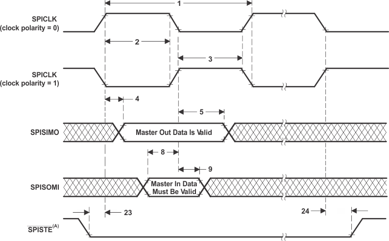
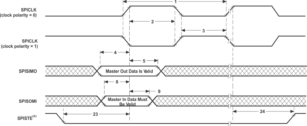
4.10.5.1.2 Non-High-Speed Slave Mode Timings
Table 4-80 lists the SPI slave mode switching characteristics. Table 4-81 lists the SPI slave mode timing requirements.
Figure 4-71 shows the SPI slave mode external timing where the clock phase = 0. Figure 4-72 shows the SPI slave mode external timing where the clock phase = 1.
Table 4-80 SPI Slave Mode Switching Characteristics
over recommended operating conditions (unless otherwise noted)| NO. | PARAMETER | MIN | MAX | UNIT | |
|---|---|---|---|---|---|
| 15 | td(SOMI)S | Delay time, SPICLK to SPISOMI valid | 20 | ns | |
| 16 | tv(SOMI)S | Valid time, SPISOMI valid after SPICLK | 0 | ns | |
Table 4-81 SPI Slave Mode Timing Requirements
| NO. | MIN | MAX | UNIT | ||
|---|---|---|---|---|---|
| 12 | tc(SPC)S | Cycle time, SPICLK | 4tc(SYSCLK) | ns | |
| 13 | tw(SPC1)S | Pulse duration, SPICLK, first pulse | 2tc(SYSCLK) – 1 | ns | |
| 14 | tw(SPC2)S | Pulse duration, SPICLK, second pulse | 2tc(SYSCLK) – 1 | ns | |
| 19 | tsu(SIMO)S | Setup time, SPISIMO valid before SPICLK | 1.5tc(SYSCLK) | ns | |
| 20 | th(SIMO)S | Hold time, SPISIMO valid after SPICLK | 1.5tc(SYSCLK) | ns | |
| 25 | tsu(STE)S | Setup time, SPISTE active before SPICLK | 1.5tc(SYSCLK) | ns | |
| 26 | th(STE)S | Hold time, SPISTE inactive after SPICLK | 1.5tc(SYSCLK) | ns | |
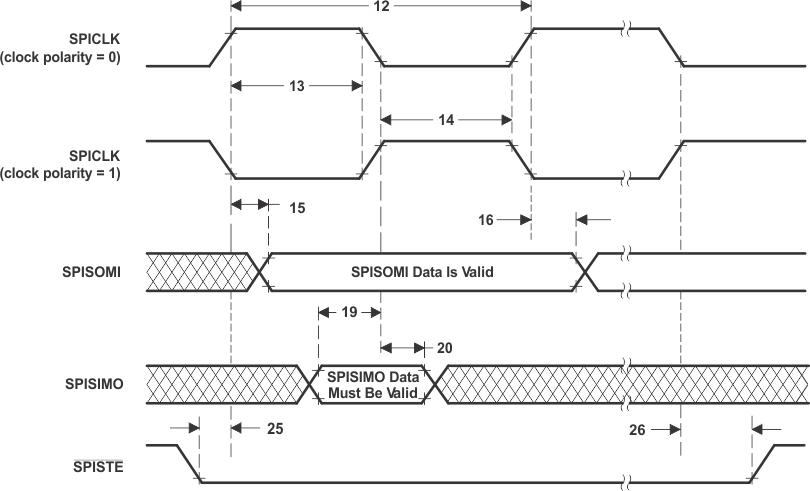 Figure 4-71 SPI Slave Mode External Timing (Clock Phase = 0)
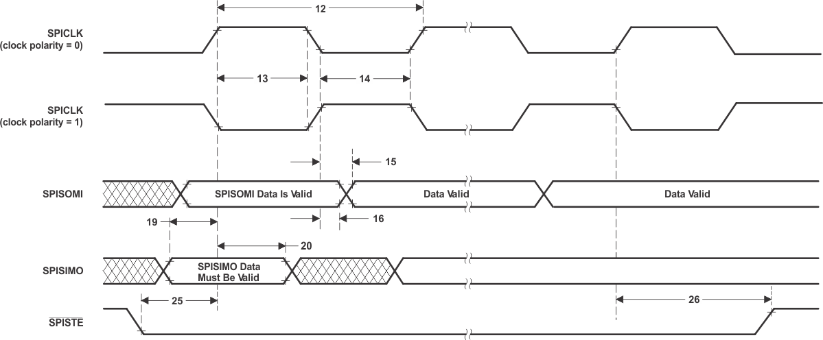 Figure 4-72 SPI Slave Mode External Timing (Clock Phase = 1)
4.10.5.1.3 High-Speed Master Mode Timings
Table 4-82 lists the SPI high-speed master mode switching characteristics where the clock phase = 0. Figure 4-73 shows the high-speed SPI master mode external timing where the clock phase = 0.
Table 4-83 lists the SPI high-speed master mode switching characteristics where the clock phase = 1. Figure 4-74 shows the high-speed SPI master mode external timing where the clock phase = 1.
Table 4-84 lists the SPI high-speed master mode timing requirements.
Table 4-82 SPI High-Speed Master Mode Switching Characteristics (Clock Phase = 0)
over recommended operating conditions (unless otherwise noted)| NO. | PARAMETER | (BRR + 1) CONDITION(1) | MIN | MAX | UNIT | |
|---|---|---|---|---|---|---|
| 1 | tc(SPC)M | Cycle time, SPICLK | Even | 4tc(LSPCLK) | 128tc(LSPCLK) | ns |
| Odd | 5tc(LSPCLK) | 127tc(LSPCLK) | ||||
| 2 | tw(SPC1)M | Pulse duration, SPICLK, first pulse | Even | 0.5tc(SPC)M – 1 | 0.5tc(SPC)M + 1 | ns |
| Odd | 0.5tc(SPC)M + 0.5tc(LSPCLK) – 1 |
0.5tc(SPC)M + 0.5tc(LSPCLK) + 1 |
||||
| 3 | tw(SPC2)M | Pulse duration, SPICLK, second pulse | Even | 0.5tc(SPC)M – 1 | 0.5tc(SPC)M + 1 | ns |
| Odd | 0.5tc(SPC)M – 0.5tc(LSPCLK) – 1 |
0.5tc(SPC)M – 0.5tc(LSPCLK) + 1 |
||||
| 4 | td(SIMO)M | Delay time, SPICLK to SPISIMO valid | Even, Odd | 1 | ns | |
| 5 | tv(SIMO)M | Valid time, SPISIMO valid after SPICLK | Even | 0.5tc(SPC)M – 1 | ns | |
| Odd | 0.5tc(SPC)M – 0.5tc(LSPCLK) – 1 |
|||||
| 23 | td(SPC)M | Delay time, SPISTE active to SPICLK | Even | tc(SPC)M – 1 | ns | |
| Odd | 0.5tc(SPC)M – 0.5tc(LSPCLK) – 1 |
|||||
| 24 | td(STE)M | Delay time, SPICLK to SPISTE inactive | Even | 0.5tc(SPC)M – 1 | ns | |
| Odd | 0.5tc(SPC)M – 0.5tc(LSPCLK) – 1 |
|||||
Table 4-83 SPI High-Speed Master Mode Switching Characteristics (Clock Phase = 1)
over recommended operating conditions (unless otherwise noted)| NO. | PARAMETER | (BRR + 1) CONDITION(1) | MIN | MAX | UNIT | |
|---|---|---|---|---|---|---|
| 1 | tc(SPC)M | Cycle time, SPICLK | Even | 4tc(LSPCLK) | 128tc(LSPCLK) | ns |
| Odd | 5tc(LSPCLK) | 127tc(LSPCLK) | ||||
| 2 | tw(SPC1)M | Pulse duration, SPICLK, first pulse | Even | 0.5tc(SPC)M – 1 | 0.5tc(SPC)M + 1 | ns |
| Odd | 0.5tc(SPC)M – 0.5tc(LSPCLK) – 1 |
0.5tc(SPC)M – 0.5tc(LSPCLK) + 1 |
||||
| 3 | tw(SPC2)M | Pulse duration, SPICLK, second pulse | Even | 0.5tc(SPC)M – 1 | 0.5tc(SPC)M + 1 | ns |
| Odd | 0.5tc(SPC)M + 0.5tc(LSPCLK) – 1 |
0.5tc(SPC)M + 0.5tc(LSPCLK) + 1 |
||||
| 4 | td(SIMO)M | Delay time, SPISIMO valid to SPICLK | Even | 0.5tc(SPC)M – 1 | ns | |
| Odd | 0.5tc(SPC)M + 0.5tc(LSPCLK) – 1 |
|||||
| 5 | tv(SIMO)M | Valid time, SPISIMO valid after SPICLK | Even | 0.5tc(SPC)M – 1 | ns | |
| Odd | 0.5tc(SPC)M – 0.5tc(LSPCLK) – 1 |
|||||
| 23 | td(SPC)M | Delay time, SPISTE active to SPICLK | Even, Odd | tc(SPC)M – 1 | ns | |
| 24 | td(STE)M | Delay time, SPICLK to SPISTE inactive | Even | 0.5tc(SPC)M – 1 | ns | |
| Odd | 0.5tc(SPC)M – 0.5tc(LSPCLK) – 1 |
|||||
Table 4-84 SPI High-Speed Master Mode Timing Requirements
| NO. | (BRR + 1) CONDITION(1) | MIN | MAX | UNIT | ||
|---|---|---|---|---|---|---|
| 8 | tsu(SOMI)M | Setup time, SPISOMI valid before SPICLK | Even, Odd | 1 | ns | |
| 9 | th(SOMI)M | Hold time, SPISOMI valid after SPICLK | Even, Odd | 5 | ns | |


4.10.5.1.4 High-Speed Slave Mode Timings
Table 4-85 lists the SPI high-speed slave mode switching characteristics. Table 4-86 lists the SPI high-speed slave mode timing requirements.
Figure 4-75 shows the high-speed SPI slave mode external timing where the clock phase = 0. Figure 4-76 shows the high-speed SPI slave mode external timing where the clock phase = 1.
Table 4-85 SPI High-Speed Slave Mode Switching Characteristics
over recommended operating conditions (unless otherwise noted)| NO. | PARAMETER | MIN | MAX | UNIT | |
|---|---|---|---|---|---|
| 15 | td(SOMI)S | Delay time, SPICLK to SPISOMI valid | 9 | ns | |
| 16 | tv(SOMI)S | Valid time, SPISOMI valid after SPICLK | 0 | ns | |
Table 4-86 SPI High-Speed Slave Mode Timing Requirements
| NO. | MIN | MAX | UNIT | ||
|---|---|---|---|---|---|
| 12 | tc(SPC)S | Cycle time, SPICLK | 4tc(SYSCLK) | ns | |
| 13 | tw(SPC1)S | Pulse duration, SPICLK, first pulse | 2tc(SYSCLK) – 1 | ns | |
| 14 | tw(SPC2)S | Pulse duration, SPICLK, second pulse | 2tc(SYSCLK) – 1 | ns | |
| 19 | tsu(SIMO)S | Setup time, SPISIMO valid before SPICLK | 1.5tc(SYSCLK) | ns | |
| 20 | th(SIMO)S | Hold time, SPISIMO valid after SPICLK | 1.5tc(SYSCLK) | ns | |
| 25 | tsu(STE)S | Setup time, SPISTE active before SPICLK | 1.5tc(SYSCLK) | ns | |
| 26 | th(STE)S | Hold time, SPISTE inactive after SPICLK | 1.5tc(SYSCLK) | ns | |
 Figure 4-75 High-Speed SPI Slave Mode External Timing (Clock Phase = 0)
 Figure 4-76 High-Speed SPI Slave Mode External Timing (Clock Phase = 1)
4.10.6 Universal Serial Bus (USB) Controller
The USB controller operates as a full-speed or low-speed function controller during point-to-point communications with USB host or device functions.
The USB module has the following features:
- USB 2.0 full-speed (12 Mbps) and low-speed (1.5 Mbps) operation
- Integrated PHY
- Three transfer types: control, interrupt, and bulk
- 32 endpoints
- One dedicated control IN endpoint and one dedicated control OUT endpoint
- 15 configurable IN endpoints and 15 configurable OUT endpoints
- 4KB of dedicated endpoint memory
Figure 4-77 shows the USB block diagram.
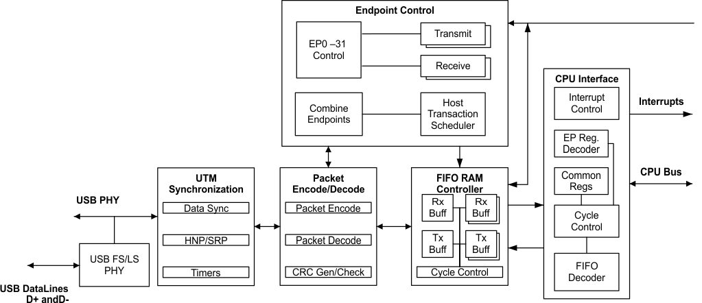 Figure 4-77 USB Block Diagram
NOTE
The accuracy of the on-chip zero-pin oscillator (Table 4-18, Internal Oscillator Electrical Characteristics) will not meet the accuracy requirements of the USB protocol. An external clock source must be used for applications using USB. For applications using the USB boot mode, see Section 5.10 (Boot ROM and Peripheral Booting) for clock frequency requirements.
4.10.6.1 USB Electrical Data and Timing
Table 4-87 shows the USB input ports DP and DM timing requirements. Table 4-88 shows the USB output ports DP and DM switching characteristics.
Table 4-87 USB Input Ports DP and DM Timing Requirements
| MIN | MAX | UNIT | ||
|---|---|---|---|---|
| V(CM) | Differential input common mode range | 0.8 | 2.5 | V |
| Z(IN) | Input impedance | 300 | kΩ | |
| VCRS | Crossover voltage | 1.3 | 2.0 | V |
| VIL | Static SE input logic-low level | 0.8 | V | |
| VIH | Static SE input logic-high level | 2.0 | V | |
| VDI | Differential input voltage | 0.2 | V | |
Table 4-88 USB Output Ports DP and DM Switching Characteristics
over recommended operating conditions (unless otherwise noted)| PARAMETER | TEST CONDITIONS | MIN | MAX | UNIT | |
|---|---|---|---|---|---|
| VOH | D+, D– single-ended | USB 2.0 load conditions | 2.8 | 3.6 | V |
| VOL | D+, D– single-ended | USB 2.0 load conditions | 0 | 0.3 | V |
| Z(DRV) | D+, D– impedance | 28 | 44 | Ω | |
| tr | Rise time | Full speed, differential, CL = 50 pF, 10%/90%, Rpu on D+ |
4 | 20 | ns |
| tf | Fall time | Full speed, differential, CL = 50 pF, 10%/90%, Rpu on D+ |
4 | 20 | ns |
4.10.7 Universal Parallel Port (uPP) Interface
The uPP interface is a high-speed parallel interface with dedicated data lines and minimal control signals. The uPP interface is designed to interface cleanly with high-speed ADCs or DACs with 8-bit data width. It can also be interconnected with field-programmable gate arrays (FPGAs) or other uPP devices to achieve high-speed digital data transfer. It can operate in receive mode or transmit mode (simplex mode).
The uPP interface includes an internal DMA controller to maximize throughput and minimize CPU overhead during high-speed data transmission. All uPP transactions use internal DMA to feed data to or retrieve data from the I/O channels. Even though there is only one I/O channel, the DMA controller includes two DMA channels to support data interleave mode, in which all DMA resources service a single I/O channel.
On this device, the uPP interface is the dedicated resource for the CPU1 subsystem. CPU1, CPU1.CLA1, and CPU1.DMA have access to this module. Two dedicated 512-byte data RAMs (also known as MSG RAMs) are tightly coupled with the uPP module (one for each, TX and RX). These data RAMs are used to store the bulk of data to avoid frequent interruptions to the CPU. Only CPU1 and CPU1.CLA1 have access to these data RAMs. Figure 4-78 shows the integration of the uPP on this device.
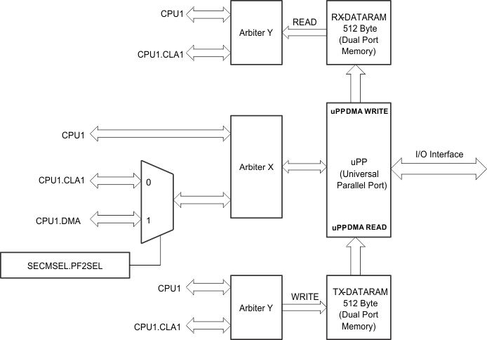 Figure 4-78 uPP Integration
NOTE
On some TI devices, the uPP module is also called the Radio Peripheral Interface (RPI) module.
The uPP interface supports the following:
- Mainstream high-speed data converters with parallel conversion interface.
- Mainstream high-speed streaming interface with frame START indication.
- Mainstream high-speed streaming interface with data ENABLE indication.
- Mainstream high-speed streaming interface with synchronization WAIT signal.
- SDR (single-data-rate) or DDR (double-data-rate, interleaved) interface.
- Multiplexing of interleaved data in SDR transmit case.
- Demultiplexing and multiplexing of interleaved data in DDR case.
- I/O interface clock frequency up to 50 MHz for SDR, and 25 MHz for DDR.
- Single-channel 8-bit input receive or output transmit mode.
- Max throughput is 50MB/s for pure read or pure write.
- Available as a DSP to FPGA general-purpose streaming interface.
Figure 4-79 shows the uPP functional block diagram.
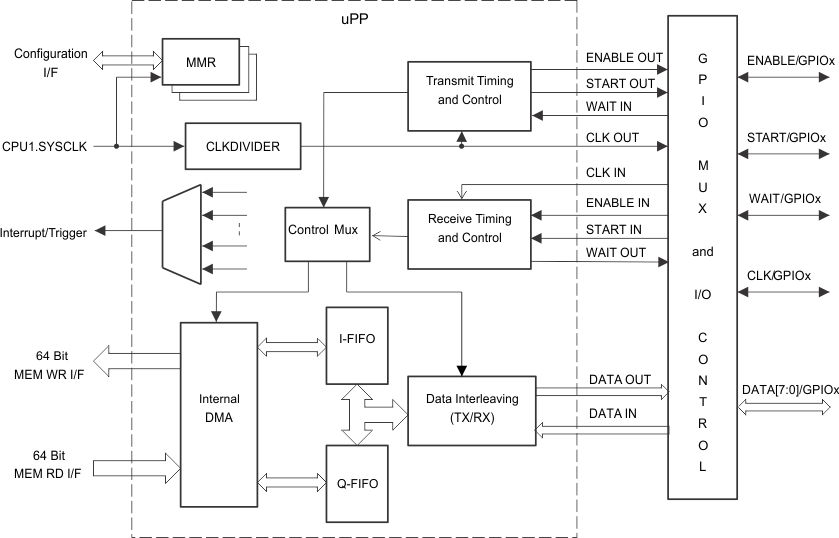 Figure 4-79 uPP Functional Block Diagram
4.10.7.1 uPP Electrical Data and Timing
Table 4-89 shows the uPP timing requirements. Table 4-90 shows the uPP switching characteristics. Figure 4-80 through Figure 4-83 show the uPP timing diagrams.
Table 4-89 uPP Timing Requirements
| NO. | MIN | MAX | UNIT | |||
|---|---|---|---|---|---|---|
| 1 | tc(CLK) | Cycle time, CLK | SDR mode | 20 | ns | |
| DDR mode | 40 | |||||
| 2 | tw(CLKH) | Pulse width, CLK high | SDR mode | 8 | ns | |
| DDR mode | 18 | |||||
| 3 | tw(CLKL) | Pulse width, CLK low | SDR mode | 8 | ns | |
| DDR mode | 18 | |||||
| 4 | tsu(STV-CLKH) | Setup time, START valid before CLK high | 4 | ns | ||
| 5 | th(CLKH-STV) | Hold time, START valid after CLK high | 0.8 | ns | ||
| 6 | tsu(ENV-CLKH) | Setup time, ENABLE valid before CLK high | 4 | ns | ||
| 7 | th(CLKH-ENV) | Hold time, ENABLE valid after CLK high | 0.8 | ns | ||
| 8 | tsu(DV-CLKH) | Setup time, DATA valid before CLK high | 4 | ns | ||
| 9 | th(CLKH-DV) | Hold time, DATA valid after CLK high | 0.8 | ns | ||
| 10 | tsu(DV-CLKL) | Setup time, DATA valid before CLK low | 4 | ns | ||
| 11 | th(CLKL-DV) | Hold time, DATA valid after CLK low | 0.8 | ns | ||
| 19 | tsu(WTV-CLKH) | Setup time, WAIT valid before CLK high | SDR mode | 20 | ns | |
| 20 | th(CLKH-WTV) | Hold time, WAIT valid after CLK high | SDR mode | 0 | ns | |
| 21 | tsu(WTV-CLKL) | Setup time, WAIT valid before CLK low | DDR mode | 20 | ns | |
| 22 | th(CLKL-WTV) | Hold time, WAIT valid after CLK low | DDR mode | 0 | ns | |
Table 4-90 uPP Switching Characteristics
over recommended operating conditions (unless otherwise noted)| NO. | PARAMETER | MIN | MAX | UNIT | ||
|---|---|---|---|---|---|---|
| 12 | tc(CLK) | Cycle time, CLK | SDR mode | 20 | ns | |
| DDR mode | 40 | |||||
| 13 | tw(CLKH) | Pulse width, CLK high | SDR mode | 8 | ns | |
| DDR mode | 18 | |||||
| 14 | tw(CLKL) | Pulse width, CLK low | SDR mode | 8 | ns | |
| DDR mode | 18 | |||||
| 15 | td(CLKH-STV) | Delay time, START valid after CLK high | 3 | 12 | ns | |
| 16 | td(CLKH-ENV) | Delay time, ENABLE valid after CLK high | 3 | 12 | ns | |
| 17 | td(CLKH-DV) | Delay time, DATA valid after CLK high | 3 | 12 | ns | |
| 18 | td(CLKL-DV) | Delay time, DATA valid after CLK low | 3 | 12 | ns | |
 Figure 4-80 uPP Single Data Rate (SDR) Receive Timing
 Figure 4-81 uPP Double Data Rate (DDR) Receive Timing
 Figure 4-82 uPP Single Data Rate (SDR) Transmit Timing
 Figure 4-83 uPP Double Data Rate (DDR) Transmit Timing