SCDS406A December 2018 – February 2024 TMUX1109
PRODUCTION DATA
- 1
- 1 Features
- 2 Applications
- 3 Description
- 4 Pin Configuration and Functions
-
5 Specifications
- 5.1 Absolute Maximum Ratings
- 5.2 ESD Ratings
- 5.3 Recommended Operating Conditions
- 5.4 Thermal Information
- 5.5 Electrical Characteristics (VDD = 5V ±10 %)
- 5.6 Electrical Characteristics (VDD = 3.3V ±10 %)
- 5.7 Electrical Characteristics (VDD = 2.5V ±10 %), (VSS = –2.5V ±10 %)
- 5.8 Electrical Characteristics (VDD = 1.8V ±10 %)
- 5.9 Electrical Characteristics (VDD = 1.2V ±10 %)
- Typical Characteristics
- 6 Detailed Description
- 7 Application and Implementation
- 8 Device and Documentation Support
- 9 Revision History
- 10Mechanical, Packaging, and Orderable Information
Package Options
Refer to the PDF data sheet for device specific package drawings
Mechanical Data (Package|Pins)
- PW|16
- RSV|16
Thermal pad, mechanical data (Package|Pins)
Orderable Information
7.4.1 Layout Guidelines
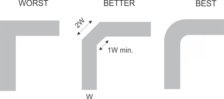
When a PCB trace turns a corner at a 90° angle, a reflection can occur. A reflection occurs primarily because of the change of width of the trace. At the apex of the turn, the trace width increases to 1.414 times the width. This increase upsets the transmission-line characteristics, especially the distributed capacitance and self–inductance of the trace which results in the reflection. Not all PCB traces can be straight and therefore some traces must turn corners. Figure 7-3 shows progressively better techniques of rounding corners. Only the last example (BEST) maintains constant trace width and minimizes reflections.
 Figure 7-3 Trace
Example
Route high-speed signals using a minimum of vias and corners which reduces signal reflections and impedance changes. When a via must be used, increase the clearance size around it to minimize its capacitance. Each via introduces discontinuities in the signal’s transmission line and increases the chance of picking up interference from the other layers of the board. Be careful when designing test points, through-hole pins are not recommended at high frequencies.
Figure 7-4 shows an example of a PCB layout with the TMUX1109. Some key considerations are:
- Decouple the VDD pin with a 0.1µF capacitor, and place the capacitor as close to the pin as possible. Ensure that the capacitor voltage rating is sufficient for the VDD supply.
- Keep the input lines as short as possible.
- Use a solid ground plane to reduce electromagnetic interference (EMI) noise pickup.
- Do not run sensitive analog traces in parallel with digital traces. Avoid crossing digital and analog traces if possible, and only make perpendicular crossings when necessary.