SCDS401C December 2018 – February 2024 TMUX1119
PRODUCTION DATA
- 1
- 1 Features
- 2 Applications
- 3 Description
- 4 Pin Configuration and Functions
-
5 Specifications
- 5.1 Absolute Maximum Ratings
- 5.2 ESD Ratings
- 5.3 Recommended Operating Conditions
- 5.4 Thermal Information
- 5.5 Electrical Characteristics (VDD = 5V ±10 %)
- 5.6 Electrical Characteristics (VDD = 3.3V ±10 %)
- 5.7 Electrical Characteristics (VDD = 1.8V ±10 %)
- 5.8 Electrical Characteristics (VDD = 1.2V ±10 %)
- Typical Characteristics
- 6 Parameter Measurement Information
- 7 Detailed Description
- 8 Application and Implementation
- 9 Device and Documentation Support
- 10Revision History
- 11Mechanical, Packaging, and Orderable Information
Package Options
Mechanical Data (Package|Pins)
Thermal pad, mechanical data (Package|Pins)
Orderable Information
7.3.6 Ultra-Low Charge Injection
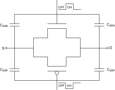
The TMUX1119 has a transmission gate topology, as shown in Figure 7-3. Any mismatch in the stray capacitance associated with the NMOS and PMOS causes an output level change whenever the switch is opened or closed.
 Figure 7-3 Transmission Gate Topology
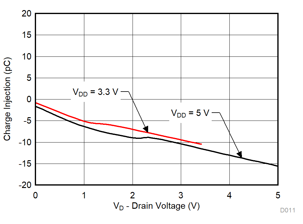
The TMUX1119 has special charge-injection cancellation circuitry that reduces the drain-to-source charge injection to -6pC at VD = 1V as shown in Figure 7-4.
 Figure 7-4 Charge Injection vs Drain Voltage