SCDS376A February 2018 – September 2018 TMUX6104
PRODUCTION DATA.
- 1 Features
- 2 Applications
- 3 Description
- 4 Revision History
- 5 Pin Configuration and Functions
-
6 Specifications
- 6.1 Absolute Maximum Ratings
- 6.2 ESD Ratings
- 6.3 Thermal Information
- 6.4 Recommended Operating Conditions
- 6.5 Electrical Characteristics (Dual Supplies: ±15 V)
- 6.6 Switching Characteristics (Dual Supplies: ±15 V)
- 6.7 Electrical Characteristics (Single Supply: 12 V)
- 6.8 Switching Characteristics (Single Supply: 12 V)
- 6.9 Typical Characteristics
- 7 Parameter Measurement Information
-
8 Detailed Description
- 8.1
Overview
- 8.1.1 On-Resistance
- 8.1.2 Off-Leakage Current
- 8.1.3 On-Leakage Current
- 8.1.4 Transition Time
- 8.1.5 Break-Before-Make Delay
- 8.1.6 Turn-On and Turn-Off Time
- 8.1.7 Charge Injection
- 8.1.8 Off Isolation
- 8.1.9 Channel-to-Channel Crosstalk
- 8.1.10 Bandwidth
- 8.1.11 THD + Noise
- 8.1.12 AC Power Supply Rejection Ratio (AC PSRR)
- 8.2 Functional Block Diagram
- 8.3 Feature Description
- 8.4 Device Functional Modes
- 8.1
Overview
- 9 Application and Implementation
- 10Power Supply Recommendations
- 11Layout
- 12Device and Documentation Support
- 13Mechanical, Packaging, and Orderable Information
Package Options
Mechanical Data (Package|Pins)
- PW|14
Thermal pad, mechanical data (Package|Pins)
Orderable Information
9.2 Typical Application
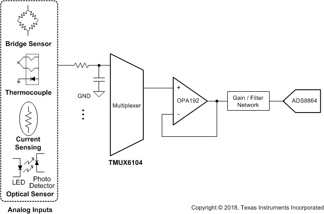
Figure 33 shows a 16-bit, differential, 4-channel, multiplexed, data-acquisition system. This example is typical in industrial applications that require low distortion and a high-voltage input. The circuit uses the ADS8864, a 16-bit, 400-kSPS successive-approximation-resistor (SAR) analog-to-digital converter (ADC), along with a precision, high-voltage, signal-conditioning front end, and a 4-channel single-ended mux. This TI Precision Design details the process for optimizing the precision, high-voltage, front-end drive circuit using the TMUX6104 and OPA192 to achieve excellent dynamic performance and linearity with the ADS8864.
 Figure 33. 16-Bit Precision Multiplexed Data-Acquisition System for High-Voltage Inputs With Lowest Distortion