SCDS376A February   2018  – September 2018 TMUX6104

PRODUCTION DATA.  

  1. Features
  2. Applications
  3. Description
    1.     Device Images
      1.      Simplified Schematic
  4. Revision History
  5. Pin Configuration and Functions
    1.     Pin Functions
  6. Specifications
    1. 6.1 Absolute Maximum Ratings
    2. 6.2 ESD Ratings
    3. 6.3 Thermal Information
    4. 6.4 Recommended Operating Conditions
    5. 6.5 Electrical Characteristics (Dual Supplies: ±15 V)
    6. 6.6 Switching Characteristics (Dual Supplies: ±15 V)
    7. 6.7 Electrical Characteristics (Single Supply: 12 V)
    8. 6.8 Switching Characteristics (Single Supply: 12 V)
    9. 6.9 Typical Characteristics
  7. Parameter Measurement Information
    1. 7.1 Truth Table
  8. Detailed Description
    1. 8.1 Overview
      1. 8.1.1  On-Resistance
      2. 8.1.2  Off-Leakage Current
      3. 8.1.3  On-Leakage Current
      4. 8.1.4  Transition Time
      5. 8.1.5  Break-Before-Make Delay
      6. 8.1.6  Turn-On and Turn-Off Time
      7. 8.1.7  Charge Injection
      8. 8.1.8  Off Isolation
      9. 8.1.9  Channel-to-Channel Crosstalk
      10. 8.1.10 Bandwidth
      11. 8.1.11 THD + Noise
      12. 8.1.12 AC Power Supply Rejection Ratio (AC PSRR)
    2. 8.2 Functional Block Diagram
    3. 8.3 Feature Description
      1. 8.3.1 Ultralow Leakage Current
      2. 8.3.2 Ultralow Charge Injection
      3. 8.3.3 Bidirectional and Rail-to-Rail Operation
    4. 8.4 Device Functional Modes
  9. Application and Implementation
    1. 9.1 Application Information
    2. 9.2 Typical Application
      1. 9.2.1 Design Requirements
      2. 9.2.2 Detailed Design Procedure
      3. 9.2.3 Application Curve
  10. 10Power Supply Recommendations
  11. 11Layout
    1. 11.1 Layout Guidelines
    2. 11.2 Layout Example
  12. 12Device and Documentation Support
    1. 12.1 Documentation Support
      1. 12.1.1 Related Documentation
    2. 12.2 Receiving Notification of Documentation Updates
    3. 12.3 Community Resources
    4. 12.4 Trademarks
    5. 12.5 Electrostatic Discharge Caution
    6. 12.6 Glossary
  13. 13Mechanical, Packaging, and Orderable Information

Package Options

Mechanical Data (Package|Pins)
Thermal pad, mechanical data (Package|Pins)
Orderable Information

Typical Characteristics

at TA = 25°C, VDD = 15 V, and VSS = –15 V (unless otherwise noted)
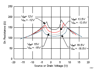
TMUX6104 D001_SCDS376.gif
TA = 25°C
Figure 1. On-Resistance vs Source or Drain Voltage
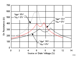
TMUX6104 D003_SCDS376.gif
TA = 25°C
Figure 3. On-Resistance vs Source or Drain Voltage
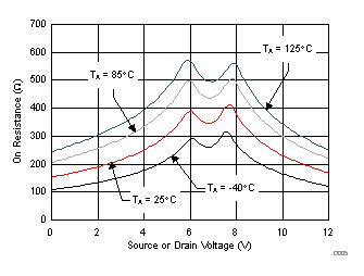
TMUX6104 D005_SCDS376.gif
VDD = 12 V, VSS = 0 V
Figure 5. On-Resistance vs Source or Drain Voltage
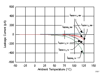
TMUX6104 D007_SCDS376.gif
VDD = 12 V, VSS = 0 V
Figure 7. Leakage Current vs Temperature
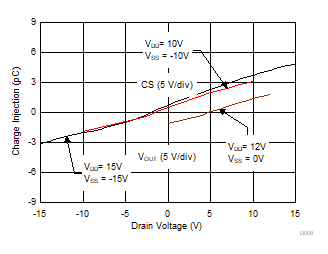
TMUX6104 D009_SCDS376.gif
Drain-to-source, TA = 25°C
Figure 9. Charge Injection vs Drain Voltage
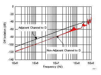
TMUX6104 D011_SCDS376.gif
VDD = 15 V, VSS = –15 V, TA = 25°C
Figure 11. Off Isolation vs Frequency
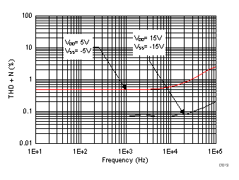
TMUX6104 D013_SCDS376.gif
TA = 25°C
Figure 13. THD+N vs Frequency
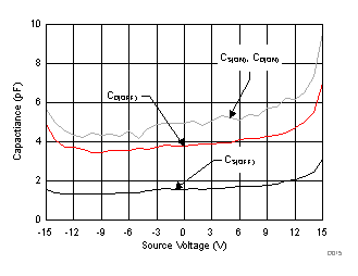
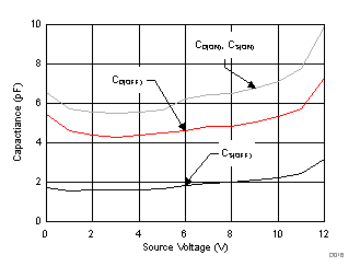
TMUX6104 D015_SCDS376.gif
VDD = 15 V, VSS = –15 V, TA = 25°C
Figure 15. Capacitance vs Source Voltage
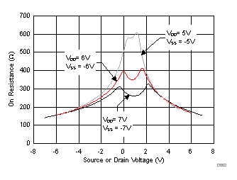
TMUX6104 D002_SCDS376.gif
TA = 25°C
Figure 2. On-Resistance vs Source or Drain Voltage
TMUX6104 D004_SCDS376.gif
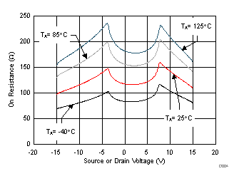
VDD = 15 V, VSS = –15 V
Figure 4. On-Resistance vs Source or Drain Voltage
TMUX6104 D006_SCDS376.gif
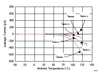
VDD = 15 V, VSS = –15 V
Figure 6. Leakage Current vs Temperature
TMUX6104 D008_SCDS376.gif
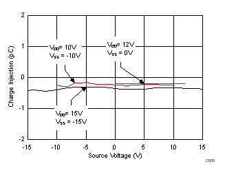
Source-to-drain, TA = 25°C
Figure 8. Charge Injection vs Source Voltage
TMUX6104 D010_SCDS376.gif
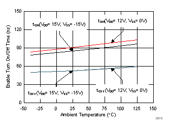
Figure 10. Turn-On and Turn-Off Times vs Temperature
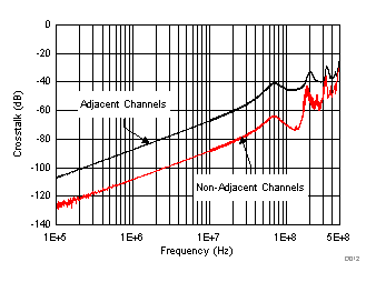
TMUX6104 D012_SCDS376.gif
VDD = 15 V, VSS = –15 V, TA = 25°C
Figure 12. Crosstalk vs Frequency
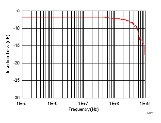
TMUX6104 D014_SCDS376.gif
VDD = 15 V, VSS = –15 V, TA = 25°C
Figure 14. On Response vs. Frequency
TMUX6104 D016_SCDS376.gif
VDD = 12 V, VSS = 0 V, TA = 25°C
Figure 16. Capacitance vs Source Voltage