SCDS418F July 2020 – July 2024 TMUX7208 , TMUX7209
PRODUCTION DATA
- 1
- 1 Features
- 2 Applications
- 3 Description
- 4 Device Comparison Table
- 5 Pin Configuration and Functions
-
6 Specifications
- 6.1 Absolute Maximum Ratings
- 6.2 ESD Ratings
- 6.3 Thermal Information
- 6.4 Recommended Operating Conditions
- 6.5 Source or Drain Continuous Current
- 6.6 ±15 V Dual Supply: Electrical Characteristics
- 6.7 ±15 V Dual Supply: Switching Characteristics
- 6.8 ±20 V Dual Supply: Electrical Characteristics
- 6.9 ±20 V Dual Supply: Switching Characteristics
- 6.10 44 V Single Supply: Electrical Characteristics
- 6.11 44 V Single Supply: Switching Characteristics
- 6.12 12 V Single Supply: Electrical Characteristics
- 6.13 12 V Single Supply: Switching Characteristics
- 6.14 Typical Characteristics
-
7 Parameter Measurement Information
- 7.1 On-Resistance
- 7.2 Off-Leakage Current
- 7.3 On-Leakage Current
- 7.4 Transition Time
- 7.5 tON(EN) and tOFF(EN)
- 7.6 Break-Before-Make
- 7.7 tON (VDD) Time
- 7.8 Propagation Delay
- 7.9 Charge Injection
- 7.10 Off Isolation
- 7.11 Crosstalk
- 7.12 Bandwidth
- 7.13 THD + Noise
- 7.14 Power Supply Rejection Ratio (PSRR)
- 8 Detailed Description
- 9 Application and Implementation
- 10Device and Documentation Support
- 11Revision History
- 12Mechanical, Packaging, and Orderable Information
Package Options
Mechanical Data (Package|Pins)
Thermal pad, mechanical data (Package|Pins)
- RUM|16
Orderable Information
9.2.2 Detailed Design Procedure
The application shown in Figure 9-2 demonstrates how a multiplexer can be used to simplify the signal chain and monitor multiple input signals to a single ADC channel. In this example the ADC (ADS8661) has software programmable input ranges up to ±12.288V. The ADC also has overvoltage protection up to ±20V which allows for the multiplexer to be powered with wider supply voltages than the input signal range to maximize on resistance performance of the multiplexer, while still maintaining system level overvoltage protection beyond the useable signal range. Both the multiplexer and the ADC are capable of operation in extended industrial temperature range of -40°C to +125°C allowing for use in a wider array of industrial systems.
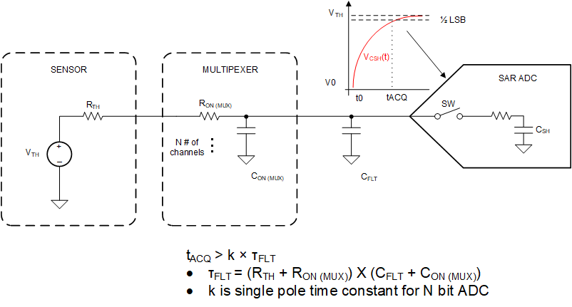
Many SAR ADCs have an analog input structure that consists of a sampling switch and a sampling capacitor. Many signal chains will have a driver amplifier to help charge the input of the ADC to meet a fast system acquisition time. However a driver amplifier is not always needed to drive SAR ADCs. Figure 9-2 shows a typical diagram of a sensor driving the SAR ADC input directly after being passed through the multiplexer. A filter capacitor (CFLT) is connected to the input of the ADC to reduce the sampling charge injection and provides a charge bucket to quickly charge the internal sample-and-hold capacitor of the ADC.
The sensor block simplifies the device into a Thevenin equivalent voltage source (VTH) and resistance (RTH) which can be extracted from the device datasheets. Similarly the multiplexer can be thought of as a series resistance (RON(MUX)) and capacitance (CON(MUX)). To ensure maximum precision of the signal chain the system should be able to settle within 1/2 of an LSB within the acquisition time of the ADC. The time constant can be calculated as shown in Figure 9-2. This equation highlights the importance of selecting a multiplexer with low on-resistance to further reduce the system time constant. Additionally low charge injection performance of the multiplexer is helpful to reduce conversion errors and improve accuracy of the measurements.
 Figure 9-2 Driving SAR ADC