SLOS520A August 2007 – March 2016 TPA2013D1
PRODUCTION DATA.
- 1 Features
- 2 Applications
- 3 Description
- 4 Revision History
- 5 Device Comparison Table
- 6 Pin Configuration and Functions
-
7 Specifications
- 7.1 Absolute Maximum Ratings
- 7.2 ESD Ratings
- 7.3 Recommended Operating Conditions
- 7.4 Thermal Information
- 7.5 DC Characteristics
- 7.6 Boost Converter DC Characteristics
- 7.7 Class D Amplifier DC Characteristics
- 7.8 AC Characteristics
- 7.9 Class D Amplifier AC Characteristics
- 7.10 Dissipation Ratings
- 7.11 Typical Characteristics
- 8 Parameter Measurement Information
- 9 Detailed Description
-
10Application and Implementation
- 10.1 Application Information
- 10.2
Typical Applications
- 10.2.1
TPA2013D1 With Differential Input Signal
- 10.2.1.1 Design Requirements
- 10.2.1.2 Detailed Design Procedure
- 10.2.1.3 Application Curves
- 10.2.2 Bypassing the Boost Converter
- 10.2.3 Stereo Operation Application
- 10.2.4 LED Driver for Digital Still Cameras
- 10.2.5 Design Requirements
- 10.2.6 Detailed Design Procedure
- 10.2.7 Application Curves
- 10.2.1
TPA2013D1 With Differential Input Signal
- 11Power Supply Recommendations
- 12Layout
- 13Device and Documentation Support
- 14Mechanical, Packaging, and Orderable Information
Package Options
Mechanical Data (Package|Pins)
Thermal pad, mechanical data (Package|Pins)
- RGP|20
Orderable Information
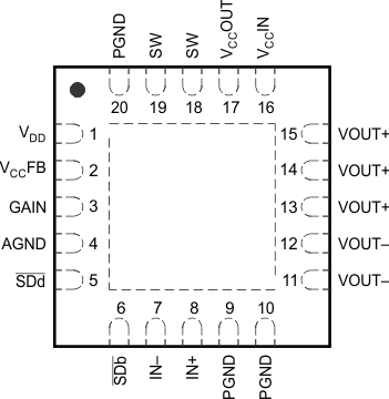
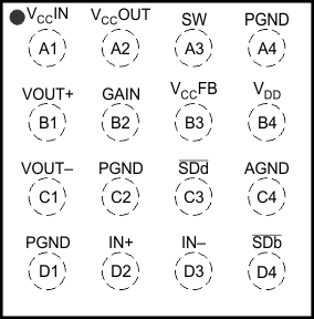
6 Pin Configuration and Functions
RGP Package
20-Pin VQFN
Top View

YZH Package
16-Pin DSBGA
Top View

Pin Functions
| PIN | I/O | DESCRIPTION | ||
|---|---|---|---|---|
| NAME | VQFN | DSBGA | ||
| AGND | 4 | C4 | – | Analog ground – connect all GND pins together |
| GAIN | 3 | B2 | I | Gain selection pin |
| IN+ | 8 | D2 | I | Positive audio input |
| IN– | 7 | D3 | I | Negative audio input |
| PGND | 9, 10, 20 | D1, C2, A4 | – | Power ground – connect all GND pins together |
| SDb | 6 | D4 | I | Shutdown terminal for the Boost Converter |
| SDd | 5 | C3 | I | Shutdown terminal for the Class D Amplifier |
| SW | 18, 19 | A3 | – | Boost and rectifying switch input |
| Thermal Pad | Die Pad | N/A | P | Solder the thermal pad on the bottom of the QFN package to the GND plane of the PCB. It is required for mechanical stability and enhances thermal performance. |
| VCCFB | 2 | B3 | I | Voltage feedback |
| VC CIN | 16 | A1 | – | Class-D audio power amplifier voltage supply – connect to VCCOUT |
| VCCOUT | 17 | A2 | – | Boost converter output – connect to VCCIN |
| VDD | 1 | B4 | – | Supply voltage |
| VOUT+ | 13, 14, 15 | B1 | O | Positive audio output |
| VOUT– | 11, 12 | C1 | O | Negative audio output |