SLOS520A August 2007 – March 2016 TPA2013D1
PRODUCTION DATA.
- 1 Features
- 2 Applications
- 3 Description
- 4 Revision History
- 5 Device Comparison Table
- 6 Pin Configuration and Functions
-
7 Specifications
- 7.1 Absolute Maximum Ratings
- 7.2 ESD Ratings
- 7.3 Recommended Operating Conditions
- 7.4 Thermal Information
- 7.5 DC Characteristics
- 7.6 Boost Converter DC Characteristics
- 7.7 Class D Amplifier DC Characteristics
- 7.8 AC Characteristics
- 7.9 Class D Amplifier AC Characteristics
- 7.10 Dissipation Ratings
- 7.11 Typical Characteristics
- 8 Parameter Measurement Information
- 9 Detailed Description
-
10Application and Implementation
- 10.1 Application Information
- 10.2
Typical Applications
- 10.2.1
TPA2013D1 With Differential Input Signal
- 10.2.1.1 Design Requirements
- 10.2.1.2 Detailed Design Procedure
- 10.2.1.3 Application Curves
- 10.2.2 Bypassing the Boost Converter
- 10.2.3 Stereo Operation Application
- 10.2.4 LED Driver for Digital Still Cameras
- 10.2.5 Design Requirements
- 10.2.6 Detailed Design Procedure
- 10.2.7 Application Curves
- 10.2.1
TPA2013D1 With Differential Input Signal
- 11Power Supply Recommendations
- 12Layout
- 13Device and Documentation Support
- 14Mechanical, Packaging, and Orderable Information
Package Options
Mechanical Data (Package|Pins)
Thermal pad, mechanical data (Package|Pins)
- RGP|20
Orderable Information
9 Detailed Description
9.1 Overview
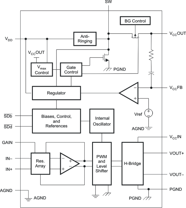
The TPA2013D1 is a high efficiency Class D audio power amplifier with an integrated boost converter. It drives up to 2.7 W (10% THD+N) into a 4-Ω speaker. The built-in boost converter generates the voltage rail for the Class-D amplifier. The TPA2013D1 has an integrated low-pass filter to improve RF rejection and reduce out-of-band noise, increasing the signal-to-noise ratio (SNR).
9.2 Functional Block Diagram

9.3 Feature Description
9.3.1 Fully Differential Amplifier
The TPA2013D1 is a fully differential amplifier with differential inputs and outputs. The fully differential amplifier consists of a differential amplifier with common-mode feedback. The differential amplifier ensures that the amplifier outputs a differential voltage on the output that is equal to the differential input times the gain. The common-mode feedback ensures that the common-mode voltage at the output is biased around VCC/2 regardless of the common-mode voltage at the input. The fully differential TPA2013D1 can still be used with a single-ended input; however, the TPA2013D1 must be used with differential inputs when in a noisy environment, like a wireless handset, to ensure maximum noise rejection.
9.3.1.1 Advantages of Fully Differential Amplifiers
- Input-coupling capacitors not required:
- The fully differential amplifier allows the inputs to be biased at voltage other than mid-supply. The inputs of the TPA2013D1 can be biased anywhere within the common mode input voltage range listed in the Recommended Operating Conditions. If the inputs are biased outside of that range, input-coupling capacitors are required.
- Midsupply bypass capacitor, C(BYPASS), not required:
- The fully differential amplifier does not require a bypass capacitor. Any shift in the midsupply affects both positive and negative channels equally and cancels at the differential output.
- Better RF-immunity:
- GSM handsets save power by turning on and shutting off the RF transmitter at a rate of 217 Hz. The transmitted signal is picked-up on input and output traces. The fully differential amplifier cancels the signal better than the typical audio amplifier.
9.3.2 Class-D Amplifier
The TPA2013D1 is a high efficiency Class-D audio power amplifier with an integrated boost converter able to drive up to 2.7 W (10% THD+N) into a 4-Ω speaker with 85% typical efficiency, the device helps extend battery life when playing audio. It is available in 2.275-mm × 2.275-mm 16-ball WCSP and 4-mm × 4-mm 20-lead QFN packages. The device has three selectable gain settings of 2 V/V, 6 V/V and 10 V/V.
9.3.3 Boost Converter
The TPA2013D1 consists of a boost converter and a Class-D amplifier. The boost converter takes a low supply voltage, VDD, and increases it to a higher output voltage, VCC.
The two main passive components necessary for the boost converter are the boost inductor and the boost capacitor. The boost inductor stores current, and the boost capacitor stores charge. As the Class-D amplifier depletes the charge in the boost capacitor, the boost inductor charges it back up with the stored current. The cycle of charge and discharge occurs at a frequency of fboost.
The TPA2013D1 allows a range of VCC voltages, including setting VCC lower than VDD.
9.3.4 Operation With DACs and CODECs
When using switching amplifiers with CODECs and DACs, sometimes there is an increase in the output noise floor from the audio amplifier. This occurs when mixing of the output frequencies of the CODEC and DAC with the switching frequencies of the audio amplifier input stage. The noise increase can be solved by placing a low-pass filter between the CODEC and DAC and audio amplifier. This filters off the high frequencies that cause the problem and allow proper performance.
The TPA2013D1 has a two pole low-pass filter at the inputs. The cutoff frequency of the filter is set to approximately 100 kHz. The integrated low-pass filter of the TPA2013D1 eliminates the need for additional external filtering components. A properly designed additional low-pass filter may be added without altering the performance of the device.
If driving the TPA2013D1 input with 4th-order or higher ΔΣ DACs or CODECs, add an R-C low-pass filter at each of the audio inputs (IN+ and IN–) of the TPA2013D1 to ensure best performance. The recommended resistor value is 100 Ω and the capacitor value of 47 nF.
9.3.5 Filter-Free Operation and Ferrite Bead Filters
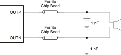
A ferrite bead filter can often be used if the design is failing radiated emissions without an LC filter and the frequency sensitive circuit is greater than 1 MHz. This filter functions well for circuits that just have to pass FCC and CE because FCC and CE only test radiated emissions greater than 30 MHz. When choosing a ferrite bead, choose one with high impedance at high frequencies, and very low impedance at low frequencies. In addition, select a ferrite bead with adequate current rating to prevent distortion of the output signal.
Use an LC output filter if there are low-frequency, (< 1 MHz) EMI-sensitive circuits and/or there are long leads from amplifier to speaker.
Figure 32 shows a typical ferrite bead output filters.
 Figure 32. Typical Ferrite Chip Bead Filter
Table 1. Suggested Chip Ferrite Bead
| LOAD | VENDOR | PART NUMBER | SIZE |
|---|---|---|---|
| 8 Ω | Murata | BLM18EG121SN1 | 0603 |
| 4 Ω | TDK | MPZ2012S101A | 0805 |
9.3.6 Fixed Gain Settings
The TPA2013D1 has 3 selectable fixed-gains: 6 dB, 15.5 dB, and 20 dB. Connect the GAIN pin as shown in Table 2.
Table 2. Amplifier Fixed-Gain
| CONNECT GAIN PIN TO | AMPLIFIER GAIN |
|---|---|
| GND | 6 dB |
| No connection (Floating) | 15.5 dB |
| VBAT | 20 dB |
9.4 Device Functional Modes
9.4.1 Boost Converter Mode
The TPA2013D1 has 4 boost converter operation modes as shown in Table 3.
Table 3. Boost Converter Mode Condition
| CASE | OUTPUT CURRENT | MODE OF OPERATION |
|---|---|---|
| VDD < VCC | Low | Continuous (fixed frequency) |
| VDD < VCC | High | Continuous (fixed frequency) |
| VDD ≥ VCC | Low | Discontinuous (variable frequency) |
| VDD ≥ VCC | High | Discontinuous (variable frequency) |
9.4.2 Shutdown Mode
The TPA2013D1 amplifier can be put in shutdown mode when asserting SDd pin to a logic LOW. While in shutdown mode, the device output stage is turned off and the current consumption is very low. The boost converter can be put in shutdown mode when asserting SDb pin to a logic LOW. While in shutdown Mode, the boost converter is turned off.
Table 4. Device Configuration
| SDb | SDd | BOOST CONVERTER | CLASS D AMPLIFIER | COMMENTS |
|---|---|---|---|---|
| low | low | OFF | OFF | Device is in shutdown mode Iq ≤ 1 μA |
| low | high | OFF | ON | Boost converter is off. Class-D Audio Power Amplifier (APA) can be driven by an external pass transistor connected to the battery. |
| high | low | ON | OFF | Class-D APA is off. Boost Converter is on and can be used to drive an external device. |
| high | high | ON | ON | Boost converter and Class-D APA are on. Normal operation. Boost converter can be used to drive an external device in parallel to the Class-D APA within the limits of the boost converter output current. |