SLOS520A August 2007 – March 2016 TPA2013D1
PRODUCTION DATA.
- 1 Features
- 2 Applications
- 3 Description
- 4 Revision History
- 5 Device Comparison Table
- 6 Pin Configuration and Functions
-
7 Specifications
- 7.1 Absolute Maximum Ratings
- 7.2 ESD Ratings
- 7.3 Recommended Operating Conditions
- 7.4 Thermal Information
- 7.5 DC Characteristics
- 7.6 Boost Converter DC Characteristics
- 7.7 Class D Amplifier DC Characteristics
- 7.8 AC Characteristics
- 7.9 Class D Amplifier AC Characteristics
- 7.10 Dissipation Ratings
- 7.11 Typical Characteristics
- 8 Parameter Measurement Information
- 9 Detailed Description
-
10Application and Implementation
- 10.1 Application Information
- 10.2
Typical Applications
- 10.2.1
TPA2013D1 With Differential Input Signal
- 10.2.1.1 Design Requirements
- 10.2.1.2 Detailed Design Procedure
- 10.2.1.3 Application Curves
- 10.2.2 Bypassing the Boost Converter
- 10.2.3 Stereo Operation Application
- 10.2.4 LED Driver for Digital Still Cameras
- 10.2.5 Design Requirements
- 10.2.6 Detailed Design Procedure
- 10.2.7 Application Curves
- 10.2.1
TPA2013D1 With Differential Input Signal
- 11Power Supply Recommendations
- 12Layout
- 13Device and Documentation Support
- 14Mechanical, Packaging, and Orderable Information
Package Options
Mechanical Data (Package|Pins)
Thermal pad, mechanical data (Package|Pins)
- RGP|20
Orderable Information
7 Specifications
7.1 Absolute Maximum Ratings
over operating free-air temperature range (unless otherwise noted)(1)| MIN | MAX | UNIT | ||
|---|---|---|---|---|
| VDD | Supply voltage | –0.3 | 6 | V |
| VI | Input voltage, Vi: SDb, SDd, IN+, IN–, VCCFB | –0.3 | VDD + 0.3 | V |
| Continuous total power dissipation | See Dissipation Ratings | |||
| TA | Operating free-air temperature | –40 | 85 | °C |
| TJ | Operating junction temperature | –40 | 150 | °C |
| Tstg | Storage temperature | –65 | 150 | °C |
(1) Stresses beyond those listed under Absolute Maximum Ratings may cause permanent damage to the device. These are stress ratings only, which do not imply functional operation of the device at these or any other conditions beyond those indicated under Recommended Operating Conditions. Exposure to absolute-maximum-rated conditions for extended periods may affect device reliability.
7.2 ESD Ratings
| VALUE | UNIT | |||
|---|---|---|---|---|
| V(ESD) | Electrostatic discharge | Human-body model (HBM), per ANSI/ESDA/JEDEC JS-001(1) | ±4000 | V |
| Charged-device model (CDM), per JEDEC specification JESD22-C101(2) | ±1500 | |||
(1) JEDEC document JEP155 states that 500-V HBM allows safe manufacturing with a standard ESD control process.
(2) JEDEC document JEP157 states that 250-V CDM allows safe manufacturing with a standard ESD control process.
7.3 Recommended Operating Conditions
| MIN | MAX | UNIT | |||
|---|---|---|---|---|---|
| VDD | Supply voltage | 1.8 | 5.5 | V | |
| VIH | High-level input voltage | SDb, SDd | 1.3 | V | |
| VIL | Low-level input voltage | SDb, SDd | 0.35 | V | |
| | IIH | | High-level input current | SDb = SDd = 5.8 V, VDD = 5.5 V, VCC = 5.5 V | 1 | μA | |
| | IIL| | Low-level input current | SDb = SDd = -0.3 V, VDD = 5.5 V, VCC = 5.5 V | 20 | μA | |
| TA | Operating free-air temperature | –40 | 85 | °C | |
7.4 Thermal Information
| THERMAL METRIC(1) | TPA2013D1 | UNIT | ||
|---|---|---|---|---|
| RGP (VQFN) | YZH (DSBGA) | |||
| 20 PINS | 16 PINS | |||
| RθJA | Junction-to-ambient thermal resistance | 34 | 70.6 | °C/W |
| RθJC(top) | Junction-to-case (top) thermal resistance | 33.4 | 0.3 | °C/W |
| RθJB | Junction-to-board thermal resistance | 10.5 | 15 | °C/W |
| ψJT | Junction-to-top characterization parameter | 0.4 | 1.8 | °C/W |
| ψJB | Junction-to-board characterization parameter | 10.5 | 14.2 | °C/W |
| RθJC(bot) | Junction-to-case (bottom) thermal resistance | 3.1 | — | °C/W |
(1) For more information about traditional and new thermal metrics, see the Semiconductor and IC Package Thermal Metrics application report, SPRA953.
7.5 DC Characteristics
TA = 25°C (unless otherwise noted)| PARAMETER | TEST CONDITIONS | MIN | TYP | MAX | UNIT | |
|---|---|---|---|---|---|---|
| VCC | Class-D audio power amplifier voltage supply range, VCCIN | 3 | 5.5 | V | ||
| ISD | Shutdown quiescent current | SDd = SDb = 0 V, VDD = 1.8 V, RL = 8 Ω | 0.04 | 1.5 | μA | |
| SDd = SDb = 0 V, VDD = 3.6 V, RL = 8 Ω | 0.04 | 1.5 | ||||
| SDd = SDb = 0 V, VDD = 4.5 V, RL = 8 Ω | 0.02 | 1.5 | ||||
| SDd = SDb = 0.35 V, VDD = 1.8 V, RL = 8 Ω | 0.03 | 1.5 | ||||
| SDd = SDb = 0.35 V, VDD = 3.6 V, RL = 8 Ω | 0.03 | 1.5 | ||||
| SDd = SDb = 0.35 V, VDD = 4.5 V, RL = 8 Ω | 0.02 | 1.5 | ||||
| IDD | Boost converter quiescent current | SDd = 0 V, SDb = 1.3 V, VDD = 3.6 V, VCC = 5.5 V, No Load, No Filter | 1.3 | mA | ||
| ICC | Class D amplifier quiescent current | VDD = 3.6, Vcc = 5.5 V, No Load, No Filter | 4.3 | 6 | mA | |
| VDD = 4.5, Vcc = 5.5 V, No Load, No Filter | 3.6 | 6 | ||||
| IDD | Boost converter and audio power amplifier quiescent current, Class D(1) | SDd = SDb = 1.3 V, VDD = 3.6 V, Vcc = 5.5 V, No Load, No Filter | 16.5 | 23 | mA | |
| SDd = SDb = 1.3V, VDD = 4.5 V, Vcc = 5.5 V, No Load, No Filter | 11 | 18.5 | ||||
| f | Boost converter switching frequency | 500 | 600 | 700 | kHz | |
| Class D switching frequency | 250 | 300 | 350 | kHz | ||
| UVLO | Under voltage lockout | 1.7 | V | |||
| GAIN | Gain input low level | Gain = 2 V/V (6 dB) | 0 | 0.35 | V | |
| Gain input mid level | Gain = 6 V/V (15.5 dB) (floating input) | 0.7 | 0.8 | 1 | V | |
| Gain input high level | Gain = 10 V/V (20 dB) | 1.35 | V | |||
| PORD | Class D Power on reset ON threshold | 2.8 | V | |||
(1) IDD is calculated using IDD = (ICC× VCC)/(VDD×η), where ICC is the class D amplifier quiescent current; η = 40%, which is the boost converter efficiency when class D amplifier has no load. To achieve the minimal 40% η, it is recommended to use the suggested inductors in table 4 and to follow the layout guidelines.
7.6 Boost Converter DC Characteristics
TA = 25°C (unless otherwise noted)| PARAMETER | TEST CONDITIONS | MIN | TYP | MAX | UNIT | |
|---|---|---|---|---|---|---|
| VCC | Output voltage range | 3 | 5.5 | V | ||
| VFB | Feedback voltage | 490 | 500 | 510 | mV | |
| IOL | Output current limit, Boost_max | 1300 | 1500 | 1700 | mA | |
| RON_PB | PMOS switch resistance | 220 | mΩ | |||
| RON_NB | NMOS resistance | 170 | mΩ | |||
| Line regulation | No Load, 1.8 V < VDD < 5.2 V, VCC = 5.5 V | 3 | mV/V | |||
| Load regulation | VDD = 3.6 V, 0 < IL < 500 mA, VCC = 5.5 V | 30 | mV/A | |||
| IL | Start-up current limit, Boost | 0.4×IBoost | mA | |||
7.7 Class D Amplifier DC Characteristics
TA = 25°C (unless otherwise noted)| PARAMETER | TEST CONDITIONS | MIN | TYP | MAX | UNIT | |
|---|---|---|---|---|---|---|
| CMR | Input common mode range | Vin = ±100 mV, VDD = 1.8 V, VCC = 3 V, RL = 8 Ω | 0.5 | 2.2 | V | |
| Vin = ±100 mV, VDD = 2.5 V, VCC = 3.6 V, RL = 8 Ω | 0.5 | 2.8 | ||||
| Vin = ±100 mV, VDD = 3.6 V, VCC = 5.5 V, RL = 8 Ω | 0.5 | 4.7 | ||||
| CMRR | Input common mode rejection | RL = 8 Ω, Vicm = 0.5 and Vicm = VCC – 0.8, differential inputs shorted | –75 | dB | ||
| VOO | Output offset voltage Class-D |
VCC = 3.6 V, Av = 2 V/V, IN+ = IN– = Vref, RL = 8 Ω | 1 | 6 | mV | |
| VCC= 3.6 V, Av = 6 V/V, IN+ = IN– = Vref, RL = 8 Ω | 1 | 6 | ||||
| VCC= 3.6 V, Av = 10 V/V, IN+ = IN– = Vref, RL = 8 Ω | 1 | 6 | ||||
| VCC = 5.5 V, Av = 2 V/V, IN+ = IN– = Vref, RL = 8 Ω | 1 | 6 | ||||
| Rin | Input Impedance | Gain = 2 V/V (6 dB) | 32 | kΩ | ||
| Gain = 6 V/V (15.5 dB) | 15 | |||||
| Gain = 10 V/V (20 dB) | 9.5 | |||||
| RDS(on) | OUTP High-side FET On-state series resistance | IOUTx = –300 mA; VCC = 3.6 V | 0.36 | Ω | ||
| OUTP Low-side FET On-state series resistance | 0.36 | |||||
| RDS(on) | OUTN High-side FET On-state series resistance | 0.36 | ||||
| OUTN Low-side FET On-state series resistance | 0.36 | |||||
| AV | Low Gain | GAIN ≤ 0.35 V | 1.8 | 2 | 2.2 | V/V |
| Mid Gain | GAIN = 0.8 V | 5.7 | 6 | 6.3 | V/V | |
| High Gain | GAIN ≥ 1.35 V | 9.5 | 10 | 10.5 | V/V | |
7.8 AC Characteristics
TA = 25°C, VDD = 3.6 V, RL = 8 Ω, L = 4.7 μH (unless otherwise noted)| PARAMETER | TEST CONDITIONS | MIN | TYP | MAX | UNIT | |
|---|---|---|---|---|---|---|
| tSTART | Start up time | 1.8 V ≤ VDD ≤ 5.5 V, CIN ≤ 1 μF | 7.5 | ms | ||
| η | Efficiency | THD+N = 1%, VCC = 5.5 V, VDD = 3.6 V, RL= 8 Ω, Pout = 1.7 W, Cboost= 47μF |
85% | |||
| THD+N = 1%, VCC = 5.5 V, VDD = 4.2 V, RL = 8 Ω, Pout = 1.7 W |
87.5% | |||||
| Thermal Shutdown | Threshold | 150 | °C | |||
7.9 Class D Amplifier AC Characteristics
TA = 25°C, VDD = 3.6V, RL = 8 Ω, L = 4.7μH (unless otherwise noted)| PARAMETER | TEST CONDITIONS | MIN | TYP | MAX | UNIT | |
|---|---|---|---|---|---|---|
| KSVR Class-D |
Output referred power supply rejection ratio | VDD = 3.6 V, VCC = 5.5V, 200 mVPP ripple, f = 217 Hz |
–95 | dB | ||
| THD+N Class-D |
Total harmonic distortion + noise | f = 1 kHz, Po = 1.7 W, VCC = 5.5 V | 1% | |||
| f = 1 kHz, Po = 1.2 W, VCC = 4.5 V | 1% | |||||
| f = 1 kHz, Po = 2.2 W, VCC = 5.5 V | 10% | |||||
| f = 1 kHz, Po = 1 W, VCC = 5.5 V | 0.1% | |||||
| Vn Class-D |
Output integrated noise floor | Av = 6 dB (2V/V) | 31 | μVrms | ||
| Output integrated noise floor A-weighted | Av = 6 dB (2V/V) | 23 | ||||
| PO | Maximum output power | THD+N = 10%, VCC = 5.5 V, VDD = 3.6 V , RL = 8 Ω | 2.2 | W | ||
| THD+N = 1%, VCC = 5.5 V, VDD = 3.6 V , RL = 8 Ω | 1.7 | |||||
| THD+N = 1%, VCC = 4.5 V, VDD = 3.6 V , RL = 8 Ω | 1.2 | |||||
| THD+N = 10%, VCC = 5.5 V, VDD = 3.6 V , RL = 4 Ω | 2.7 | |||||
| THD+N = 1%, VCC = 5.5 V, VDD = 3.6 V , RL = 4 Ω | 2.2 | |||||
| THD+N = 1%, VCC = 4.5 V, VDD = 3.6 V , RL = 4 Ω | 1.9 | |||||
7.10 Dissipation Ratings
| PACKAGE | TA ≤ 25°C | DERATING FACTOR(1) | TA = 70°C | TA = 85°C |
|---|---|---|---|---|
| 16 ball WCSP | 1.5 W | 12.4 mW/°C | 1 W | 0.8 W |
| 20 pin QFN | 2.5 W | 20.1 mW/°C | 1.6 W | 1.3 W |
(1) Derating factor measured with JEDEC High K board.
7.11 Typical Characteristics
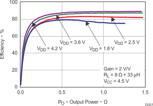 Figure 1. Efficiency vs Output Power
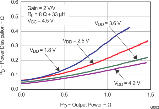 Figure 3. Power Dissipation vs Output Power
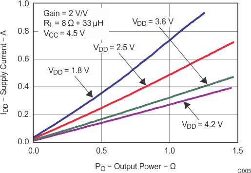 Figure 5. Supply Current vs Output Power
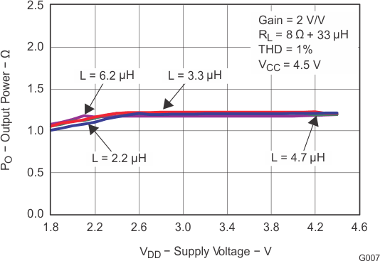 Figure 7. Output Power vs Supply Voltage
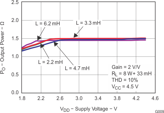 Figure 9. Output Power vs Supply Voltage
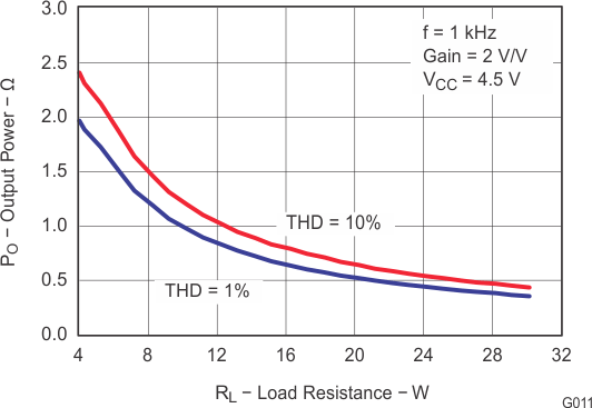 Figure 11. Output Power vs Load
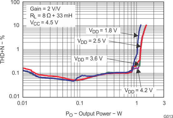 Figure 13. Total Harmonic distortion + Noise vs Output Power
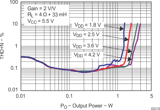 Figure 15. Total Harmonic Distortion + Noise vs Output Power
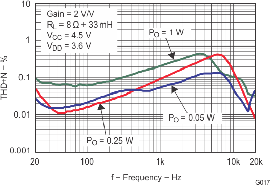 Figure 17. Total Harmonic Distortion + Noise vs Frequency
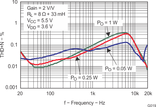 Figure 19. Total Harmonic Distortion + Noise vs Frequency
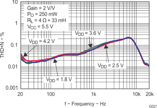 Figure 21. Total Harmonic Distortion + Noise vs Frequency
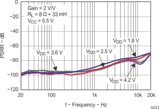 Figure 23. Power Supply Rejection Ratio vs Frequency
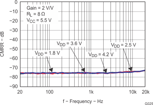 Figure 25. Common-Mode Rejection Ratio vs Frequency
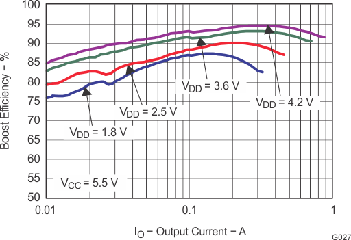 Figure 27. Boost Efficiency vs Output Current
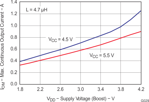 Figure 29. Maximum Continuous Output Current vs Supply Voltage (Boost)
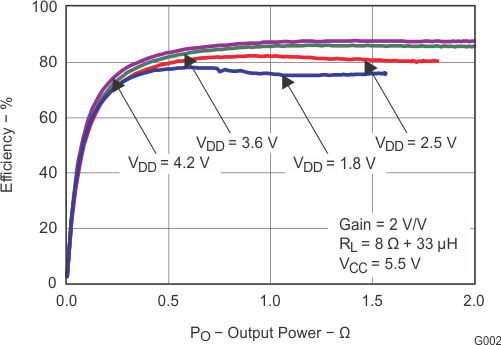 Figure 2. Efficiency vs Output Power
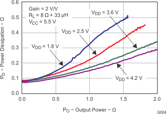 Figure 4. Power Dissipation vs Output Power
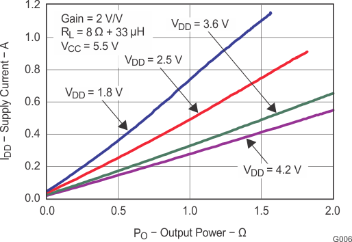 Figure 6. Supply Current vs Output Power
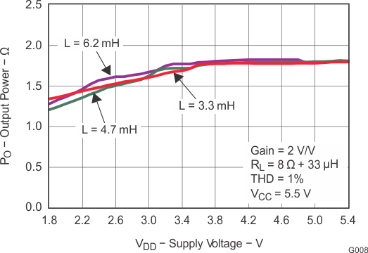 Figure 8. Output Power vs Supply Voltage
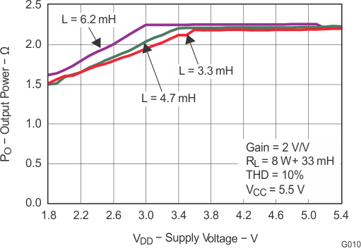 Figure 10. Output Power vs Supply Voltage
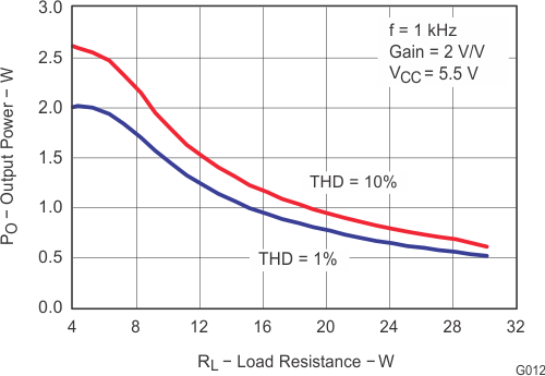 Figure 12. Output Power vs Load
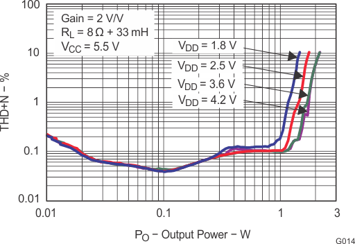 Figure 14. Total Harmonic Distortion + Noise vs Output Power
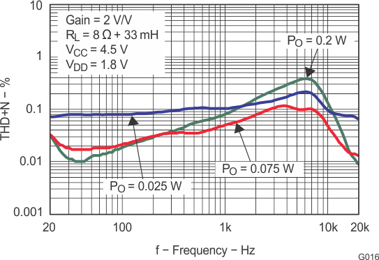 Figure 16. Total Harmonic Distortion + Noise vs Frequency
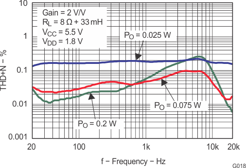 Figure 18. Total Harmonic Distortion + Noise vs Frequency
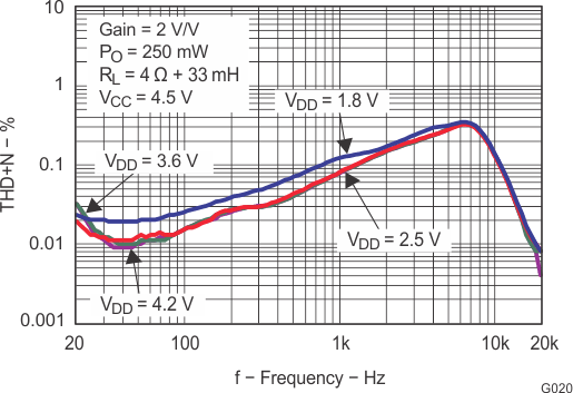 Figure 20. Total Harmonic Distortion + Noise vs Frequency
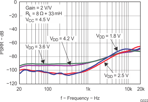 Figure 22. Power Supply Rejection Ratio vs Frequency
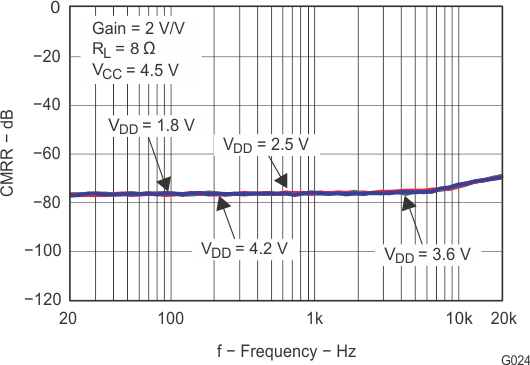 Figure 24. Common-Mode Rejection Ratio vs Frequency
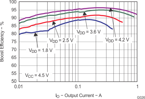 Figure 26. Boost Efficiency vs Output Current
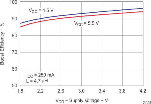 Figure 28. Boost Efficiency vs Supply Voltage
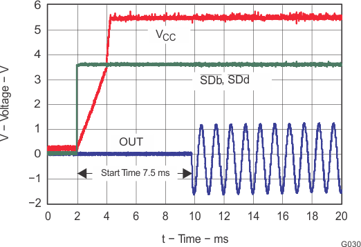 Figure 30. Start-Up Time