SLOS528F July 2009 – April 2017 TPA3110D2
PRODUCTION DATA.
- 1 Features
- 2 Applications
- 3 Description
- 4 Revision History
- 5 Device Comparison Table
- 6 Pin Configuration and F unctions
- 7 Specifications
- 8 Parameter Measurement Information
-
9 Detailed Description
- 9.1 Overview
- 9.2 Functional Block Diagram
- 9.3 Feature Description
- 9.4 Device Functional Modes
- 10Application and Implementation
- 11Power Supply Recommendations
- 12Layout
- 13Device and Documentation Support
- 14Mechanical, Packaging, and Orderable Information
Package Options
Mechanical Data (Package|Pins)
- PWP|28
Thermal pad, mechanical data (Package|Pins)
- PWP|28
Orderable Information
7 Specifications
7.1 Absolute Maximum Ratings
over operating free-air temperature range (unless otherwise noted)(1)| MIN | MAX | UNIT | |||
|---|---|---|---|---|---|
| VCC | Supply voltage | AVCC, PVCC | –0.3 V | 30 V | V |
| VI | Interface pin voltage | SD, GAIN0, GAIN1, PBTL, FAULT (2) | –0.3 V | VCC + 0.3 V | V |
| < 10 V/ms | |||||
| PLIMIT | –0.3 | GVDD + 0.3 | V | ||
| RINN, RINP, LINN, LINP | –0.3 | 6.3 | V | ||
| Continuous total power dissipation | See Thermal Information | ||||
| RL | Minimum Load Resistance | BTL: PVCC > 15 V | 4.8 | ||
| BTL: PVCC ≤ 15 V | 3.2 | ||||
| PBTL | 3.2 | ||||
| TA | Operating free-air temperature | –40 | 85 | °C | |
| TJ | Operating junction temperature range(3) | –40 | 150 | °C | |
| Tstg | Storage temperature | –65 | 150 | °C | |
(1) Stresses beyond those listed under Absolute Maximum Ratings may cause permanent damage to the device. These are stress ratings only, which do not imply functional operation of the device at these or any other conditions beyond those indicated under Recommended Operating Conditions. Exposure to absolute-maximum-rated conditions for extended periods may affect device reliability.
(2) The voltage slew rate of these pins must be restricted to no more than 10 V/ms. For higher slew rates, use a 100-kΩ resister in series with the pins.
(3) The TPA3110D2 incorporates an exposed thermal pad on the underside of the chip. This acts as a heatsink, and it must be connected to a thermally dissipating plane for proper power dissipation. Failure to do so may result in the device going into thermal protection shutdown. See TI Technical Briefs SLMA002 for more information about using the TSSOP thermal pad.
7.2 ESD Ratings
| VALUE | UNIT | |||
|---|---|---|---|---|
| V(ESD) | Electrostatic discharge | Human-body model (HBM), per ANSI/ESDA/JEDEC JS-001(1) | ±2000 | V |
| Charged-device model (CDM), per JEDEC specification JESD22-C101(2) | ±500 | |||
(1) JEDEC document JEP155 states that 500-V HBM allows safe manufacturing with a standard ESD control process.
(2) JEDEC document JEP157 states that 250-V CDM allows safe manufacturing with a standard ESD control process.
7.3 Recommended Operating Conditions
over operating free-air temperature range (unless otherwise noted)| MIN | MAX | UNIT | |||
|---|---|---|---|---|---|
| VCC | Supply voltage | PVCC, AVCC | 8 | 26 | V |
| VIH | High-level input voltage | SD, GAIN0, GAIN1, PBTL | 2 | V | |
| VIL | Low-level input voltage | SD, GAIN0, GAIN1, PBTL | 0.8 | V | |
| VOL | Low-level output voltage | FAULT, RPULL-UP= 100 k, VCC= 26 V | 0.8 | V | |
| IIH | High-level input current | SD, GAIN0, GAIN1, PBTL, VI = 2 V, VCC = 18 V | 50 | µA | |
| IIL | Low-level input current | SD, GAIN0, GAIN1, PBTL, VI = 0.8 V, VCC = 18 V | 5 | µA | |
| TA | Operating free-air temperature | –40 | 85 | °C | |
7.4 Thermal Information
| THERMAL METRIC(1) | TPA3110D2 | UNIT | |
|---|---|---|---|
| PWP (HTSSOP) | |||
| 28 PINS | |||
| RθJA | Junction-to-ambient thermal resistance | 30.3 | °C/W |
| RθJC(top) | Junction-to-case (top) thermal resistance | 33.5 | °C/W |
| RθJB | Junction-to-board thermal resistance | 17.5 | °C/W |
| ψJT | Junction-to-top characterization parameter | 0.9 | °C/W |
| ψJB | Junction-to-board characterization parameter | 7.2 | °C/W |
| RθJC(bot) | Junction-to-case (bottom) thermal resistance | 0.9 | °C/W |
(1) For more information about traditional and new thermal metrics, see the Semiconductor and IC Package Thermal Metrics application report, SPRA953.
7.5 DC Characteristics: 24 V
TA = 25°C, VCC = 24 V, RL = 8 Ω (unless otherwise noted)| PARAMETER | TEST CONDITIONS | MIN | TYP | MAX | UNIT | ||
|---|---|---|---|---|---|---|---|
| | VOS | | Class-D output offset voltage (measured differentially) | VI = 0 V, Gain = 36 dB | 1.5 | 15 | mV | ||
| ICC | Quiescent supply current | SD = 2 V, no load, PVCC = 24 V | 32 | 50 | mA | ||
| ICC(SD) | Quiescent supply current in shutdown mode | SD = 0.8 V, no load, PVCC = 24 V | 250 | 400 | µA | ||
| rDS(on) | Drain-source on-state resistance | VCC = 12 V, IO = 500 mA, TJ = 25°C |
High Side | 240 | mΩ | ||
| Low side | 240 | ||||||
| G | Gain | GAIN1 = 0.8 V | GAIN0 = 0.8 V | 19 | 20 | 21 | dB |
| GAIN0 = 2 V | 25 | 26 | 27 | ||||
| GAIN1 = 2 V | GAIN0 = 0.8 V | 31 | 32 | 33 | dB | ||
| GAIN0 = 2 V | 35 | 36 | 37 | ||||
| ton | Turn-on time | SD = 2 V | 14 | ms | |||
| tOFF | Turn-off time | SD = 0.8 V | 2 | μs | |||
| GVDD | Gate Drive Supply | IGVDD = 100 μA | 6.4 | 6.9 | 7.4 | V | |
| tDCDET | DC Detect time | V(RINN) = 6 V, VRINP = 0 V | 420 | ms | |||
7.6 DC Characteristics: 12 V
TA = 25°C, VCC = 12 V, RL = 8 Ω (unless otherwise noted)| PARAMETER | TEST CONDITIONS | MIN | TYP | MAX | UNIT | ||
|---|---|---|---|---|---|---|---|
| | VOS | | Class-D output offset voltage (measured differentially) | VI = 0 V, Gain = 36 dB | 1.5 | 15 | mV | ||
| ICC | Quiescent supply current | SD = 2 V, no load, PVCC = 12V | 20 | 35 | mA | ||
| ICC(SD) | Quiescent supply current in shutdown mode | SD = 0.8 V, no load, PVCC = 12V | 200 | µA | |||
| rDS(on) | Drain-source on-state resistance | VCC = 12 V, IO = 500 mA, TJ = 25°C |
High Side | 240 | mΩ | ||
| Low side | 240 | ||||||
| G | Gain | GAIN1 = 0.8 V | GAIN0 = 0.8 V | 19 | 20 | 21 | dB |
| GAIN0 = 2 V | 25 | 26 | 27 | ||||
| GAIN1 = 2 V | GAIN0 = 0.8 V | 31 | 32 | 33 | dB | ||
| GAIN0 = 2 V | 35 | 36 | 37 | ||||
| tON | Turn-on time | SD = 2 V | 14 | ms | |||
| tOFF | Turn-off time | SD = 0.8 V | 2 | μs | |||
| GVDD | Gate Drive Supply | IGVDD = 2 mA | 6.4 | 6.9 | 7.4 | V | |
| VO | Output Voltage maximum under PLIMIT control | V(PLIMIT) = 2 V; VI = 1 V rms | 6.75 | 7.90 | 8.75 | V | |
7.7 AC Characteristics: 24 V
TA = 25°C, VCC = 24 V, RL = 8 Ω (unless otherwise noted)| PARAMETER | TEST CONDITIONS | MIN | TYP | MAX | UNIT | |
|---|---|---|---|---|---|---|
| KSVR | Power Supply ripple rejection | 200 mVPP ripple at 1 kHz, Gain = 20 dB, Inputs ac-coupled to AGND |
–70 | dB | ||
| PO | Continuous output power | THD+N = 10%, f = 1 kHz, VCC = 16 V | 15 | W | ||
| THD+N | Total harmonic distortion + noise | VCC = 16 V, f = 1 kHz, PO = 7.5 W (half-power) | 0.1% | |||
| Vn | Output integrated noise | 20 Hz to 22 kHz, A-weighted filter, Gain = 20 dB | 65 | µV | ||
| –80 | dBV | |||||
| Crosstalk | VO = 1 Vrms, Gain = 20 dB, f = 1 kHz | –100 | dB | |||
| SNR | Signal-to-noise ratio | Maximum output at THD+N < 1%, f = 1 kHz, Gain = 20 dB, A-weighted |
102 | dB | ||
| fOSC | Oscillator frequency | 250 | 310 | 350 | kHz | |
| Thermal trip point | 150 | °C | ||||
| Thermal hysteresis | 15 | °C | ||||
7.8 AC Characteristics: 12 V
TA = 25°C, VCC = 12 V, RL = 8 Ω (unless otherwise noted)| PARAMETER | TEST CONDITIONS | MIN | TYP | MAX | UNIT | |
|---|---|---|---|---|---|---|
| KSVR | Supply ripple rejection | 200 mVPP ripple from 20 Hz–1 kHz, Gain = 20 dB, Inputs ac-coupled to AGND |
–70 | dB | ||
| PO | Continuous output power | THD+N = 10%, f = 1 kHz; VCC = 13 V | 10 | W | ||
| THD+N | Total harmonic distortion + noise | RL = 8 Ω, f = 1 kHz, PO = 5 W (half-power) | 0.06% | |||
| Vn | Output integrated noise | 20 Hz to 22 kHz, A-weighted filter, Gain = 20 dB | 65 | µV | ||
| –80 | dBV | |||||
| Crosstalk | Po = 1 W, Gain = 20 dB, f = 1 kHz | –100 | dB | |||
| SNR | Signal-to-noise ratio | Maximum output at THD+N < 1%, f = 1 kHz, Gain = 20 dB, A-weighted |
102 | dB | ||
| fOSC | Oscillator frequency | 250 | 310 | 350 | kHz | |
| Thermal trip point | 150 | °C | ||||
| Thermal hysteresis | 15 | °C | ||||
7.9 Typical Characteristics
All Measurements taken at 1 kHz, unless otherwise noted. Measurements were made using the TPA3110D2 EVM which is available at www.ti.com.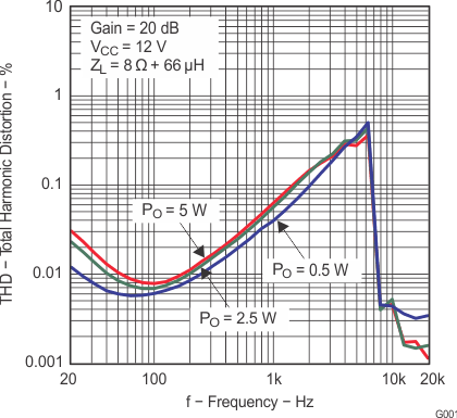 Figure 1. Total Harmonic Distortion vs Frequency (BTL)
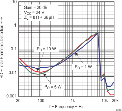 Figure 3. Total Harmonic Distortion vs Frequency (BTL)
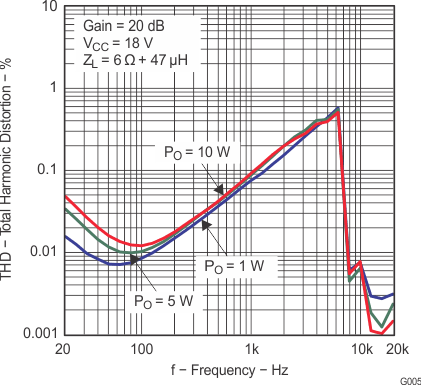 Figure 5. Total Harmonic Distortion vs Frequency (BTL)
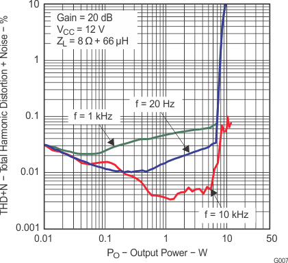 Figure 7. Total Harmonic Distortion + Noise vs Output Power (BTL)
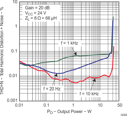 Figure 9. Total Harmonic Distortion + Noise vs Output Power (BTL)
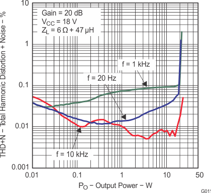 Figure 11. Total Harmonic Distortion + Noise vs Output Power (BTL)
SPACE
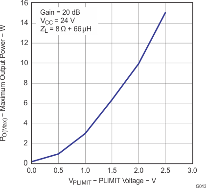
Figure 13. Maximum Output Power vs PLIMIT Voltage (BTL)
SPACE
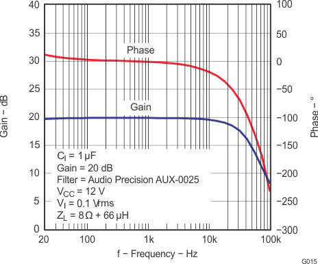
Figure 15. Gain and Phase vs Frequency (BTL)
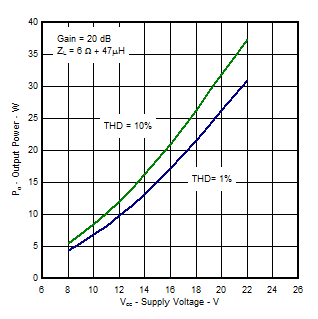 Figure 17. Output Power vs Supply Voltage (BTL)
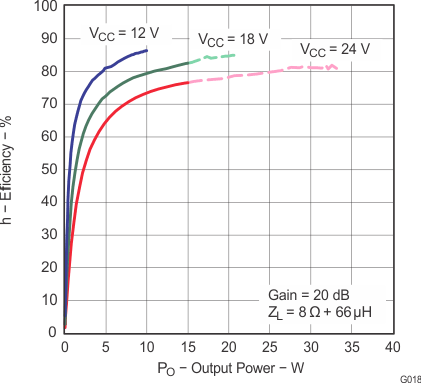
Note: Dashed Lines represent thermally limited regions.
Figure 19. Efficiency vs Output Power (BTL)
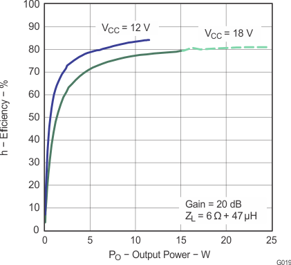
Note: Dashed Lines represent thermally limited regions.
Figure 21. Efficiency vs Output Power (BTL)
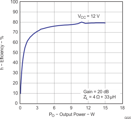 Figure 23. Efficiency vs Output Power (BTL)
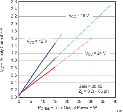
Note: Dashed Lines represent thermally limited regions.
Figure 25. Supply Current vs Total Output Power (BTL)
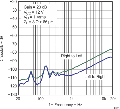
SPACE
Figure 27. Crosstalk vs Frequency (BTL)
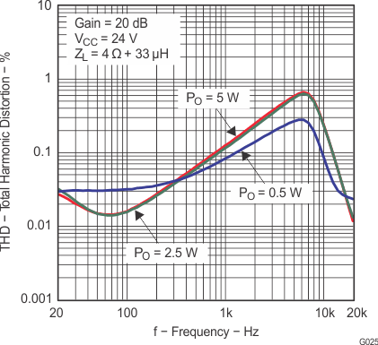 Figure 29. Total Harmonic Distortion vs Frequency (PBTL)
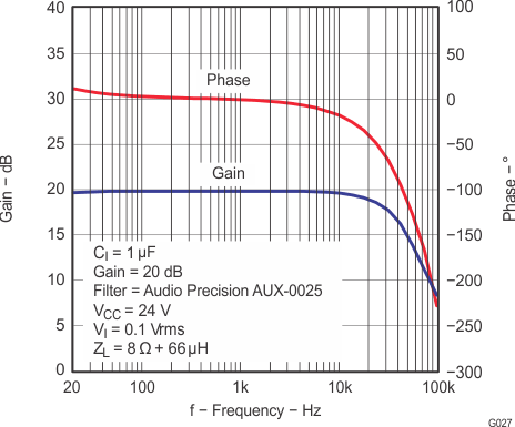 Figure 31. Gain and Phase vs Frequency (PBTL)
SPACE
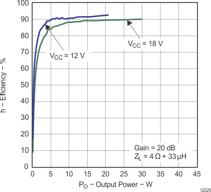
Figure 33. Efficiency vs Output Power (PBTL)
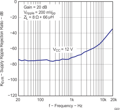 Figure 35. Supply Ripple Rejection Ratio vs Frequency (PBTL)
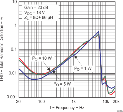 Figure 2. Total Harmonic Distortion vs Frequency (BTL)
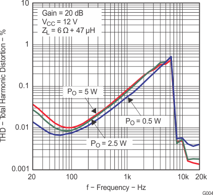 Figure 4. Total Harmonic Distortion vs Frequency (BTL)
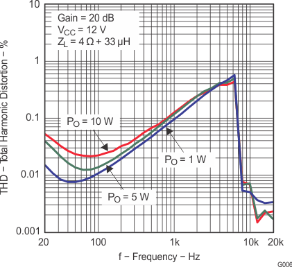 Figure 6. Total Harmonic Distortion vs Frequency (BTL)
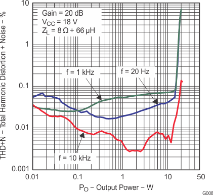 Figure 8. Total Harmonic Distortion + Noise vs Output Power (BTL)
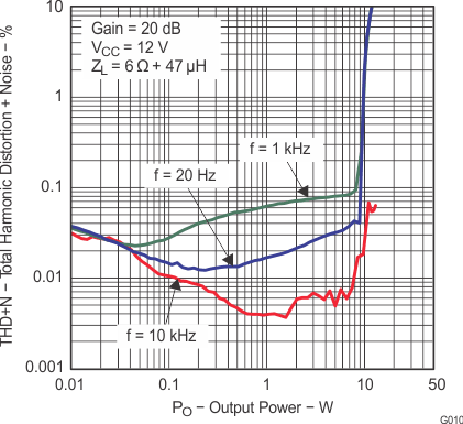 Figure 10. Total Harmonic Distortion + Noise vs Output Power (BTL)
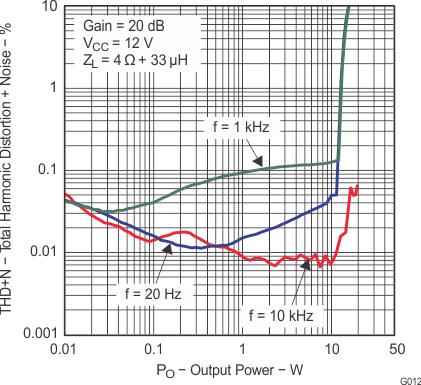 Figure 12. Total Harmonic Distortion + Noise vs Output Power (BTL)
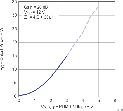
Note: Dashed Lines represent thermally limited regions.
Figure 14. Output Power vs PLIMIT Voltage (BTL)
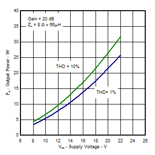 Figure 16. Output Power vs Supply Voltage (BTL)
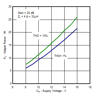
1. The figure is measured with heatsink(1) on EVM(2)
Figure 18. Output Power vs Supply Voltage (BTL)
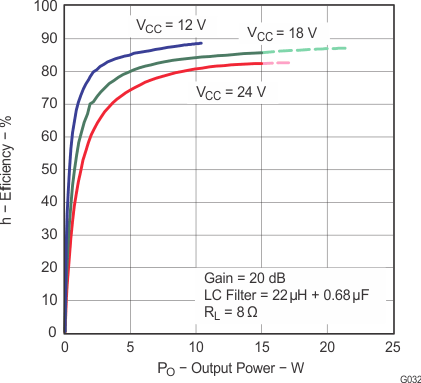
SPACE
Figure 20. Efficiency vs Output Power (BTL With LC Filter)
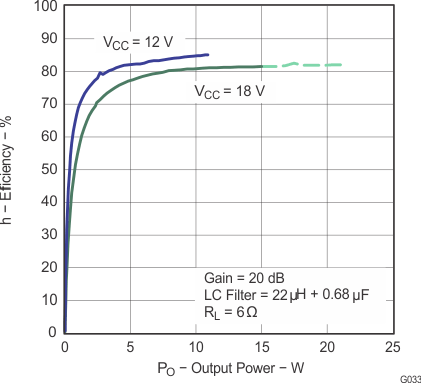 Figure 22. Efficiency vs Output Power (BTL With LC Filter)
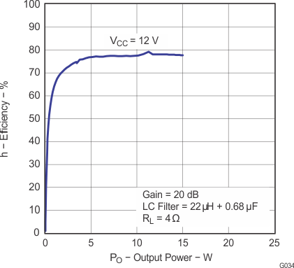
SPACE
Figure 24. Efficiency vs Output Power (BTL With LC Filter)
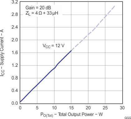
Note: Dashed Lines represent thermally limited regions.
Figure 26. Supply Current vs Total Output Power (BTL)
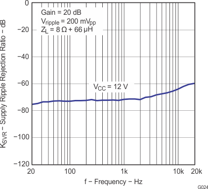 Figure 28. Supply Ripple Rejection Ratio vs Frequency (BTL)
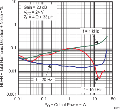 Figure 30. Total Harmonic Distortion + Noise vs Output Power (PBTL)
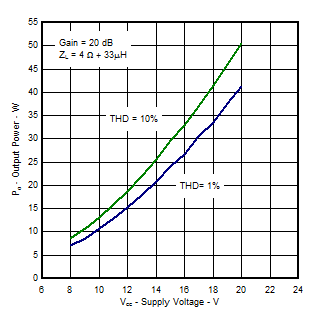
1. The figure is measured with heatsink(1) on EVM(2)
Figure 32. Output Power vs Supply Voltage (PBTL)
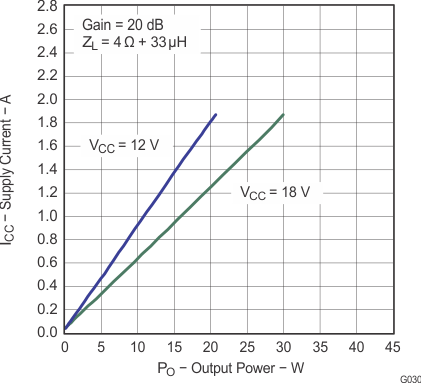 Figure 34. Supply Current vs Output Power (PBTL)
2.