SBOS496B March 2020 – February 2024 TPA6211T-Q1
PRODUCTION DATA
- 1
- 1 Features
- 2 Applications
- 3 Description
- 4 Pin Configuration and Functions
- 5 Specifications
- 6 Detailed Description
-
7 Application and Implementation
- 7.1 Application Information
- 7.2
Typical Applications
- 7.2.1
Typical Differential Input Application
- 7.2.1.1 Design Requirements
- 7.2.1.2 Detailed Design Procedure
- 7.2.1.3 Application Curves
- 7.2.2 Other Application Circuits
- 7.2.1
Typical Differential Input Application
- 8 Power Supply Recommendations
- 9 Layout
- 10Device and Documentation Support
- 11Revision History
- 12Mechanical, Packaging, and Orderable Information
Package Options
Mechanical Data (Package|Pins)
- DGN|8
Thermal pad, mechanical data (Package|Pins)
- DGN|8
Orderable Information
7.2.1.2.3 Input Capacitor (CI)
The TPA6211T-Q1 device does not require input coupling capacitors when driven by a differential input source biased from 0.5 V to VDD – 0.8 V. Use 1% tolerance or better gain-setting resistors if not using input coupling capacitors.
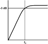
In the single-ended input application, an input capacitor (CI) is required to allow the amplifier to bias the input signal to the proper DC level. In this case, CI and RI form a high-pass filter with the corner frequency defined in Equation 19.

 Figure 7-2 Input Filter Cutoff Frequency
The value of CI is an important consideration, as it directly affects the bass (low frequency) performance of the circuit. Consider the example where RI is 10 kΩ and the specification calls for a flat bass response down to 100 Hz. Equation 19 is reconfigured as Equation 20.

In this example, CI is 0.16 µF, so the likely choice ranges from 0.22 µF to 0.47 µF. TI recommends the use of ceramic capacitors because they are the best choice in preventing leakage current. When polarized capacitors are used, the positive side of the capacitor faces the amplifier input in most applications. The input DC level is held at VDD / 2, typically higher than the source DC level. Confirming the capacitor polarity in the application is important.