SBOS496B March 2020 – February 2024 TPA6211T-Q1
PRODUCTION DATA
- 1
- 1 Features
- 2 Applications
- 3 Description
- 4 Pin Configuration and Functions
- 5 Specifications
- 6 Detailed Description
-
7 Application and Implementation
- 7.1 Application Information
- 7.2
Typical Applications
- 7.2.1
Typical Differential Input Application
- 7.2.1.1 Design Requirements
- 7.2.1.2 Detailed Design Procedure
- 7.2.1.3 Application Curves
- 7.2.2 Other Application Circuits
- 7.2.1
Typical Differential Input Application
- 8 Power Supply Recommendations
- 9 Layout
- 10Device and Documentation Support
- 11Revision History
- 12Mechanical, Packaging, and Orderable Information
Package Options
Mechanical Data (Package|Pins)
- DGN|8
Thermal pad, mechanical data (Package|Pins)
- DGN|8
Orderable Information
6.3.2 Fully Differential Amplifier Efficiency and Thermal Information
Class-AB amplifiers are inefficient, primarily because of voltage drop across the output-stage transistors. The two components of this internal voltage drop are the headroom or DC voltage drop that varies inversely to output power, and the sinewave nature of the output. The total voltage drop can be calculated by subtracting the RMS value of the output voltage from VDD. The internal voltage drop multiplied by the average value of the supply current, IDD(avg), determines the internal power dissipation of the amplifier.
An easy-to-use equation to calculate efficiency starts out as being equal to the ratio of power from the power supply to the power delivered to the load. To accurately calculate the RMS and average values of power in the load and in the amplifier, the current and voltage waveform shapes must first be understood (see Figure 6-1).
 Figure 6-1 Voltage and Current Waveforms for BTL Amplifiers
Although the voltages and currents for SE and BTL are sinusoidal in the load, currents from the supply are different between SE and BTL configurations. In an SE application the current waveform is a half-wave rectified shape, whereas in BTL the current waveform is a full-wave rectified waveform. This means RMS conversion factors are different. Keep in mind that for most of the waveform both the push and pull transistors are not on at the same time, which supports the fact that each amplifier in the BTL device only draws current from the supply for half the waveform. Equation 1 to Equation 10 are the basis for calculating amplifier efficiency.
where
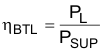
- ŋBTL is the efficiency of a BTL amplifier
- PL is the power delivered to load
- PSUP is the power drawn from power supply
PL is calculated with Equation 2, and VLRMS is calculated with Equation 3.

where
- VLRMS = RMS voltage on BTL load
- RL is load resistance
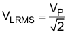
where
- VP is peak voltage on BTL load
Therefore, PL can be given as Equation 4.

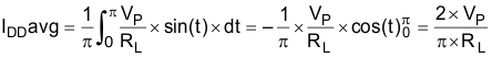
PSUP is calculated with Equation 5.
where
- VDD is power supply voltge
- IDDavg is average current drawn from the power supply
IDDavg is calculated with Equation 6.
Therefore, PSUP can be given as Equation 7.

Substituting for PL and PSUP, Equation 1 becomes Equation 8

VP is calculated with Equation 9.

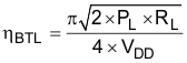
And substituting for VP, ŋBTL can be calculated with Equation 10
A simple formula for calculating the maximum power dissipated (PDmax) can be used for a differential output application:

| OUTPUT POWER | EFFICIENCY | INTERNAL DISSIPATION | POWER FROM SUPPLY | MAX AMBIENT TEMPERATURE |
|---|---|---|---|---|
| 5-V, 3-Ω SYSTEMS | ||||
| 0.5 W | 27.2% | 1.34 W | 1.84 W | 54°C |
| 1 W | 38.4% | 1.6 W | 2.6 W | 35°C |
| 2.45 W | 60.2% | 1.62 W | 4.07 W | 34°C |
| 3.1 W | 67.7% | 1.48 W | 4.58 W | 44°C |
| 5-V, 4-Ω BTL SYSTEMS | ||||
| 0.5 W | 31.4% | 1.09 W | 1.59 W | 72°C |
| 1 W | 44.4% | 1.25 W | 2.25 W | 60°C |
| 2 W | 62.8% | 1.18 W | 3.18 W | 65°C |
| 2.8 W | 74.3% | 0.97 W | 3.77 W | 80°C |
| 5-V, 8-Ω SYSTEMS | ||||
| 0.5 W | 44.4% | 0.625 W | 1.13 W | 105°C (limited by maximum ambient temperature specification) |
| 1 W | 62.8% | 0.592 W | 1.6 W | 105°C (limited by maximum ambient temperature specification) |
| 1.36 W | 73.3% | 0.496 W | 1.86 W | 105°C (limited by maximum ambient temperature specification) |
| 1.7 W | 81.9% | 0.375 W | 2.08 W | 105°C (limited by maximum ambient temperature specification) |
Equation 10 is used to calculate efficiencies for four different output power levels, see Table 6-1. The efficiency of the amplifier is quite low for lower power levels and rises sharply as power to the load is increased resulting in a nearly flat internal power dissipation over the normal operating range. The internal dissipation at full output power is less than in the half power range. Calculating the efficiency for a specific system is the key to proper power supply design. For a 2.8-W audio system with 4-Ω loads and a 5-V supply, the maximum draw on the power supply is almost 3.8 W.
A final point to remember about Class-AB amplifiers is how to manipulate the terms in the efficiency equation to the utmost advantage when possible. In Equation 10, VDD is in the denominator. This indicates that as VDD goes down, efficiency goes up.
The maximum ambient temperature depends on the heat sinking ability of the PCB system. Given RθJA (junction-to-ambient thermal resistance), the maximum allowable junction temperature, and the internal dissipation at 1-W output power with a 4-Ohm load, the maximum ambient temperature can be calculated with Equation 12. The maximum recommended junction temperature for the TPA6211T-Q1 device is 150°C.

Equation 12 shows that the maximum ambient temperature is 60°C at 1-W output power and 4-Ohm load with a 5-V supply.
Table 6-1 shows that the thermal performance must be considered when using a Class-AB amplifier to keep junction temperatures in the specified range. The TPA6211T-Q1 device is designed with thermal protection that turns the device off when the junction temperature surpasses 150°C to prevent damage to the IC. In addition, using speakers with an impedance higher than 4 Ω dramatically increases the thermal performance by reducing the output current.