SLLSE74D June 2011 – July 2016 TPD12S015A
PRODUCTION DATA.
- 1 Features
- 2 Applications
- 3 Description
- 4 Revision History
- 5 Pin Configuration and Functions
-
6 Specifications
- 6.1 Absolute Maximum Ratings
- 6.2 ESD Ratings
- 6.3 Recommended Operating Conditions
- 6.4 Thermal Information
- 6.5 Electrical Characteristics: ICC
- 6.6 Electrical Characteristics: High-Speed ESD Lines: Dx, CLK
- 6.7 Electrical Characteristics: DC-DC Converter
- 6.8 Electrical Characteristics: Passive Components
- 6.9 Electrical Characteristics: Voltage Level Shifter: SCL, SDA Lines (x_A/x_B Ports)
- 6.10 Electrical Characteristics: Voltage Level Shifter: CEC Lines (x_A/x_B Ports)
- 6.11 Electrical Characteristics: Voltage Level Shifter: HPD Line (x_A/x_B Ports)
- 6.12 Electrical Characteristics: LS_OE, CT_CP_HPD
- 6.13 Electrical Characteristics: I/O Capacitance
- 6.14 Switching Characteristics
- 6.15 Switching Characteristics: Voltage Level Shifter: SCL, SDA Lines (x_A & x_B ports); VCCA = 1.2 V
- 6.16 Switching Characteristics: Voltage Level Shifter: CEC Line (x_A & x_B ports); VCCA = 1.2 V
- 6.17 Switching Characteristics: Voltage Level Shifter: HPD Line (x_A & x_B ports); VCCA = 1.2 V
- 6.18 Switching Characteristics: Voltage Level Shifter: SCL, SDA Lines (x_A & x_B ports); VCCA = 1.5 V
- 6.19 Switching Characteristics: Voltage Level Shifter: CEC Line (x_A & x_B ports); VCCA = 1.5 V
- 6.20 Switching Characteristics: Voltage Level Shifter: HPD Line (x_A & x_B ports); VCCA = 1.5 V
- 6.21 Switching Characteristics: Voltage Level Shifter: SCL, SDA Lines (x_A & x_B ports); VCCA = 1.8 V
- 6.22 Switching Characteristics: Voltage Level Shifter: CEC Line (x_A & x_B ports); VCCA = 1.8 V
- 6.23 Switching Characteristics: Voltage Level Shifter: HPD Line (x_A & x_B ports); VCCA = 1.8 V
- 6.24 Switching Characteristics: Voltage Level Shifter: SCL, SDA Lines (x_A & x_B ports); VCCA = 2.5 V
- 6.25 Switching Characteristics: Voltage Level Shifter: CEC Line (x_A & x_B ports); VCCA = 2.5 V
- 6.26 Switching Characteristics: Voltage Level Shifter: HPD Line (x_A & x_B ports); VCCA = 2.5 V
- 6.27 Switching Characteristics: Voltage Level Shifter: SCL, SDA Lines (x_A & x_B ports); VCCA = 3.3 V
- 6.28 Switching Characteristics: Voltage Level Shifter: CEC Line (x_A & x_B ports); VCCA = 3.3 V
- 6.29 Switching Characteristics: Voltage Level Shifter: HPD Line (x_A & x_B ports); VCCA = 3.3 V
- 6.30 Typical Characteristics
- 7 Parameter Measurement Information
- 8 Detailed Description
- 9 Application and Implementation
- 10Power Supply Recommendations
- 11Layout
- 12Device and Documentation Support
- 13Mechanical, Packaging, and Orderable Information
Package Options
Mechanical Data (Package|Pins)
- YFF|28
Thermal pad, mechanical data (Package|Pins)
Orderable Information
9 Application and Implementation
NOTE
Information in the following applications sections is not part of the TI component specification, and TI does not warrant its accuracy or completeness. TI’s customers are responsible for determining suitability of components for their purposes. Customers must validate and test their design implementation to confirm system functionality.
9.1 Application Information
The TPD12S015A is an integrated solution for HDMI 1.3/1.4 interface. The device has a boost converter on the power supply, signal conditioning circuits on CEC, SCL, SDA, HPD lines, and ESD protection on the TMDS lines. To get the best performance, see Design Requirements, Detailed Design Procedure, and Application Curves.
9.2 Typical Applications
Some HDMI controller chips may have two GPIOs to control the HDMI interface chip. Figure 17 shows how TPD12S015A is used in this situation. Whereas some HDMI driver chips may have only one GPIO(CT_CP_HPD) available. In this situation, LE_OE pin is tied to HPD_A instead. Figure 18 shows how TPD12S015A is used in this situation.
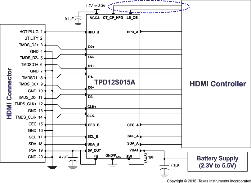 Figure 17. Application Schematics for HDMI Controllers With Two GPIOs for HDMI Interface Control
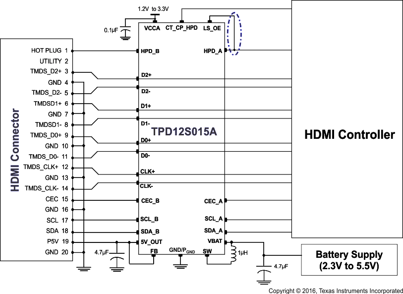 Figure 18. Application Schematics for HDMI Controllers With One GPIO for HDMI Interface Control
9.2.1 Design Requirements
Table 3 lists the known system parameters for an HDMI 1.3/1.4 application.
Table 3. Design Parameters
| DESIGN PARAMETER | VALUE |
|---|---|
| 5V_OUT DC current | 55 mA |
| CEC_A, HPD_A, SCL_A, SDA_A voltage level | VCCA |
| HDMI data rate per TMDS signal pair | 3.4 Gbps |
| Required IEC 61000-4-2 ESD Protection | ±8-kV Contact |
9.2.2 Detailed Design Procedure
9.2.2.1 Inductor Selection
To make sure that the TPD12S015A devices can operate, an inductor must be connected between pin VBAT and pin SW. A boost converter normally requires two main passive components for storing energy during the conversion. A boost inductor and a storage capacitor at the output are required. To select the boost inductor, TI recommends keeping the possible peak inductor current below the current limit threshold of the power switch in the chosen configuration. The highest peak current through the inductor and the switch depends on the output load, the input (VBAT), and the output voltage (5VOUT). Use Equation 1 to estimate the maximum average inductor current.

For example, for an output current of 55 mA at 5VOUT, approximately 150 mA of average current flows through the inductor at a minimum input voltage of 2.3 V.
The second parameter for choosing the inductor is the desired current ripple in the inductor. Normally, it is advisable to work with a ripple of less than 20% of the average inductor current. A smaller ripple reduces the magnetic hysteresis losses in the inductor, as well as output voltage ripple and EMI. However, in the same way, regulation time at load changes rises. In addition, a larger inductor increases the total system size and cost. With these parameters, it is possible to calculate the value of the minimum inductance by using Equation 2.

where
- f is the switching frequency
- ΔIL is the ripple current in the inductor, that is, 20% × IL
With this calculated value and the calculated currents, it is possible to choose a suitable inductor. In typical applications, TI recommends 1-µH inductance. The device has been optimized to operate with inductance values between 1 µH and 1.3 µH. TI recommends using at least 1-µH inductance, even if Equation 2 yields something lower. Take care so that load transients and losses in the circuit can lead to higher currents as estimated in Equation 3. Also, the losses in the inductor caused by magnetic hysteresis losses and copper losses are a major parameter for total circuit efficiency.
With the chosen inductance value, the peak current for the inductor in steady state operation can be calculated. Equation 3 shows how to calculate the peak current I.

where
This would be the critical value for the current rating for selecting the inductor. It also must be considered that load transients and error conditions may cause higher inductor currents.
9.2.2.2 Input Capacitor
Because of the nature of the boost converter having a pulsating input current, a low ESR input capacitor is required to prevent large voltage transients that can cause misbehavior of the device or interferences with other circuits in the system. TI recommends at least a 1.2-µF input capacitor to improve transient behavior of the regulator and EMI behavior of the total power supply circuit. TI recommends placing a ceramic capacitor as close as possible to the VIN and GND pins; to improve the input noise filter, it is better to use a 4.7-µF capacitor.
9.2.2.3 Output Capacitor
For the output capacitor, TI recommends using small ceramic capacitors placed as close as possible to the VOUT and GND pins of the IC. If, for any reason, the application requires the use of large capacitors, which cannot be placed close to the IC, TI recommends using a smaller ceramic capacitor in parallel to the large one. This small capacitor must be placed as close as possible to the VOUT and GND pins of the IC. To get an estimate of the recommended minimum output capacitance, use Equation 4.

where
- f is the switching frequency
- ΔV is the maximum allowed ripple
With a chosen ripple voltage of 10 mV, a minimum effective capacitance of 2.7 µF is needed. The total ripple is larger due to the ESR of the output capacitor. This additional component of the ripple can be calculated using Equation 5.
A capacitor with a value in the range of the calculated minimum must be used. This is required to maintain control loop stability. There are no additional requirements regarding minimum ESR. There is no upper limit for the output capacitance value. Larger capacitors cause lower output voltage ripple as well as lower output voltage drop during load transients.
Note that ceramic capacitors have a DC Bias effect, which will have a strong influence on the final effective capacitance needed. Therefore, the right capacitor value must be chosen very carefully. Package size and voltage rating in combination with material are responsible for differences between the rated capacitor value and the effective capacitance. The minimum effective capacitance value must be 1.2 µF, but the preferred value is about 4.7 µF.
Table 4. Passive Components: Recommended Minimum Effective Values
| COMPONENT | MIN | TARGET | MAX | UNIT |
|---|---|---|---|---|
| CIN | 1.2 | 4.7 | 6.5 | µF |
| COUT | 1.2 | 4.7 | 10 | µF |
| LIN | 0.7 | 1 | 1.3 | µH |
9.2.2.4 CEC, HPD, SCL, SDA Level Shifting Function
To accommodate for the lower logic levels of some processors' control lines, level shifters are needed to translate the interface voltage down to VCCA, the voltage level used by the processor. The TPD12S015A has bidirectional level shifters on CEC, SCL, SDA lines to support the two-way communication. The pullup resistors are integrated to minimize the number of external components. For HPD line, only one way of hot-plug indication is needed, the level shifter is unidirectional. There is a built-in HPD_B pulldown resistor to keep the voltage level low on the connector side when nothing is attached. Apart from the signal level translation, the rise-time accelerators on the connector side increases the load driving capability.
9.2.2.5 ESD
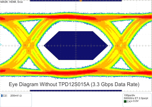
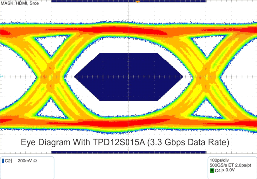
To get the best ESD performance on the interface side pins, high performance ESD diodes are needed. The TPD12S015A's ESD diodes on D0+, D0-, D1+, D1-, D2+, D2-, CLK+, CLK-, SCL_B, SDA_B, CEC_B, HPD_B, 5VOUT, FB ensure passing 8-kV contact IEC, the highest level ESD. Signal integrity on TMDS lines is also a design concern that needs to be evaluated to meet the HDMI 1.3/1.4 data rate. With the typical I/O capacitance of 1.3 pF and a bandwidth above 3 GHz, Figure 12 shows that TPD12S015A's ESD structure has enough margin to meet the data rate requirement of HDMI 1.3/1.4.
9.2.2.6 Ground Offset Consideration
Ground offset between the TPD12S015A ground and the ground of devices on port A of the TPD12S015A must be avoided. The reason for this cautionary remark is that a CMOS/NMOS open-drain capable of sinking 3 mA of current at 0.4 V has an output resistance of 133 Ω or less. Such a driver shares enough current with the port A output pulldown of the TPD12S015A to be seen as a LOW as long as the ground offset is zero. If the ground offset is greater than 0 V, then the driver resistance must be less. Because VILC can be as low as 90 mV at cold temperatures and the low end of the current distribution, the maximum ground offset must not exceed 50 mV. Bus repeaters that use an output offset are not interoperable with the port A of the TPD12S015A as their output LOW levels are not recognized by the TPD12S015A as a LOW. If the TPD12S015A is placed in an application where the VIL of port A of the TPD12S015A does not go below its VILC, it pulls port B LOW initially when port A input transitions LOW but the port B returns HIGH, so it does not reproduce the port A input on port B. Such applications must be avoided. Port B is interoperable with all I2C bus slaves, masters, and repeaters.
9.2.3 Application Curves
