SLLSE74D June 2011 – July 2016 TPD12S015A
PRODUCTION DATA.
- 1 Features
- 2 Applications
- 3 Description
- 4 Revision History
- 5 Pin Configuration and Functions
-
6 Specifications
- 6.1 Absolute Maximum Ratings
- 6.2 ESD Ratings
- 6.3 Recommended Operating Conditions
- 6.4 Thermal Information
- 6.5 Electrical Characteristics: ICC
- 6.6 Electrical Characteristics: High-Speed ESD Lines: Dx, CLK
- 6.7 Electrical Characteristics: DC-DC Converter
- 6.8 Electrical Characteristics: Passive Components
- 6.9 Electrical Characteristics: Voltage Level Shifter: SCL, SDA Lines (x_A/x_B Ports)
- 6.10 Electrical Characteristics: Voltage Level Shifter: CEC Lines (x_A/x_B Ports)
- 6.11 Electrical Characteristics: Voltage Level Shifter: HPD Line (x_A/x_B Ports)
- 6.12 Electrical Characteristics: LS_OE, CT_CP_HPD
- 6.13 Electrical Characteristics: I/O Capacitance
- 6.14 Switching Characteristics
- 6.15 Switching Characteristics: Voltage Level Shifter: SCL, SDA Lines (x_A & x_B ports); VCCA = 1.2 V
- 6.16 Switching Characteristics: Voltage Level Shifter: CEC Line (x_A & x_B ports); VCCA = 1.2 V
- 6.17 Switching Characteristics: Voltage Level Shifter: HPD Line (x_A & x_B ports); VCCA = 1.2 V
- 6.18 Switching Characteristics: Voltage Level Shifter: SCL, SDA Lines (x_A & x_B ports); VCCA = 1.5 V
- 6.19 Switching Characteristics: Voltage Level Shifter: CEC Line (x_A & x_B ports); VCCA = 1.5 V
- 6.20 Switching Characteristics: Voltage Level Shifter: HPD Line (x_A & x_B ports); VCCA = 1.5 V
- 6.21 Switching Characteristics: Voltage Level Shifter: SCL, SDA Lines (x_A & x_B ports); VCCA = 1.8 V
- 6.22 Switching Characteristics: Voltage Level Shifter: CEC Line (x_A & x_B ports); VCCA = 1.8 V
- 6.23 Switching Characteristics: Voltage Level Shifter: HPD Line (x_A & x_B ports); VCCA = 1.8 V
- 6.24 Switching Characteristics: Voltage Level Shifter: SCL, SDA Lines (x_A & x_B ports); VCCA = 2.5 V
- 6.25 Switching Characteristics: Voltage Level Shifter: CEC Line (x_A & x_B ports); VCCA = 2.5 V
- 6.26 Switching Characteristics: Voltage Level Shifter: HPD Line (x_A & x_B ports); VCCA = 2.5 V
- 6.27 Switching Characteristics: Voltage Level Shifter: SCL, SDA Lines (x_A & x_B ports); VCCA = 3.3 V
- 6.28 Switching Characteristics: Voltage Level Shifter: CEC Line (x_A & x_B ports); VCCA = 3.3 V
- 6.29 Switching Characteristics: Voltage Level Shifter: HPD Line (x_A & x_B ports); VCCA = 3.3 V
- 6.30 Typical Characteristics
- 7 Parameter Measurement Information
- 8 Detailed Description
- 9 Application and Implementation
- 10Power Supply Recommendations
- 11Layout
- 12Device and Documentation Support
- 13Mechanical, Packaging, and Orderable Information
Package Options
Mechanical Data (Package|Pins)
- YFF|28
Thermal pad, mechanical data (Package|Pins)
Orderable Information
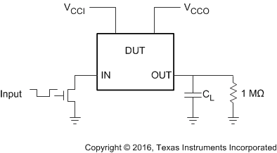
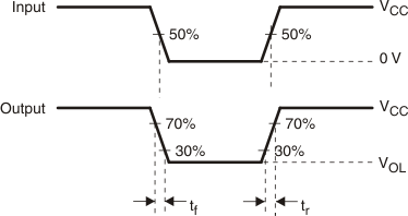
7 Parameter Measurement Information

| PIN | CL |
|---|---|
| DDC, CEC (A side) | 750 pF |
| DDC, CEC, HPD (B side) | 15 pF |

A. RT termination resistance must be equal to ZOUT of pulse generators.
B. CL includes probe and jig capacitance.
C. All input pulses are supplied by generators having the following characteristics: PRR ≤ 10 MHz, ZO = 50 Ω, slew rate ≥ 1 V/ns.
D. The outputs are measured one at a time, with one transition per measurement.
E. tPLH and tPHL are the same as tpd.
Figure 14. Test Circuit and Voltage Waveforms