SLLSE74D June 2011 – July 2016 TPD12S015A
PRODUCTION DATA.
- 1 Features
- 2 Applications
- 3 Description
- 4 Revision History
- 5 Pin Configuration and Functions
-
6 Specifications
- 6.1 Absolute Maximum Ratings
- 6.2 ESD Ratings
- 6.3 Recommended Operating Conditions
- 6.4 Thermal Information
- 6.5 Electrical Characteristics: ICC
- 6.6 Electrical Characteristics: High-Speed ESD Lines: Dx, CLK
- 6.7 Electrical Characteristics: DC-DC Converter
- 6.8 Electrical Characteristics: Passive Components
- 6.9 Electrical Characteristics: Voltage Level Shifter: SCL, SDA Lines (x_A/x_B Ports)
- 6.10 Electrical Characteristics: Voltage Level Shifter: CEC Lines (x_A/x_B Ports)
- 6.11 Electrical Characteristics: Voltage Level Shifter: HPD Line (x_A/x_B Ports)
- 6.12 Electrical Characteristics: LS_OE, CT_CP_HPD
- 6.13 Electrical Characteristics: I/O Capacitance
- 6.14 Switching Characteristics
- 6.15 Switching Characteristics: Voltage Level Shifter: SCL, SDA Lines (x_A & x_B ports); VCCA = 1.2 V
- 6.16 Switching Characteristics: Voltage Level Shifter: CEC Line (x_A & x_B ports); VCCA = 1.2 V
- 6.17 Switching Characteristics: Voltage Level Shifter: HPD Line (x_A & x_B ports); VCCA = 1.2 V
- 6.18 Switching Characteristics: Voltage Level Shifter: SCL, SDA Lines (x_A & x_B ports); VCCA = 1.5 V
- 6.19 Switching Characteristics: Voltage Level Shifter: CEC Line (x_A & x_B ports); VCCA = 1.5 V
- 6.20 Switching Characteristics: Voltage Level Shifter: HPD Line (x_A & x_B ports); VCCA = 1.5 V
- 6.21 Switching Characteristics: Voltage Level Shifter: SCL, SDA Lines (x_A & x_B ports); VCCA = 1.8 V
- 6.22 Switching Characteristics: Voltage Level Shifter: CEC Line (x_A & x_B ports); VCCA = 1.8 V
- 6.23 Switching Characteristics: Voltage Level Shifter: HPD Line (x_A & x_B ports); VCCA = 1.8 V
- 6.24 Switching Characteristics: Voltage Level Shifter: SCL, SDA Lines (x_A & x_B ports); VCCA = 2.5 V
- 6.25 Switching Characteristics: Voltage Level Shifter: CEC Line (x_A & x_B ports); VCCA = 2.5 V
- 6.26 Switching Characteristics: Voltage Level Shifter: HPD Line (x_A & x_B ports); VCCA = 2.5 V
- 6.27 Switching Characteristics: Voltage Level Shifter: SCL, SDA Lines (x_A & x_B ports); VCCA = 3.3 V
- 6.28 Switching Characteristics: Voltage Level Shifter: CEC Line (x_A & x_B ports); VCCA = 3.3 V
- 6.29 Switching Characteristics: Voltage Level Shifter: HPD Line (x_A & x_B ports); VCCA = 3.3 V
- 6.30 Typical Characteristics
- 7 Parameter Measurement Information
- 8 Detailed Description
- 9 Application and Implementation
- 10Power Supply Recommendations
- 11Layout
- 12Device and Documentation Support
- 13Mechanical, Packaging, and Orderable Information
Package Options
Mechanical Data (Package|Pins)
- YFF|28
Thermal pad, mechanical data (Package|Pins)
Orderable Information
8 Detailed Description
8.1 Overview
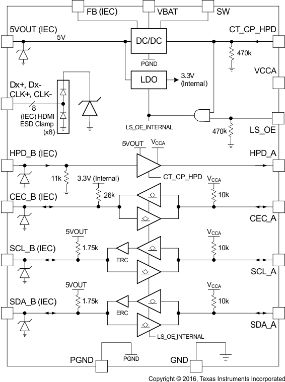
The TPD12S015A is an integrated interface solution for HDMI 1.3/1.4 interfaces, for both portable and non-portable electronics applications. It has a boost DC-DC converter that uses the 2.3-V to 5.5-V internal power supply and outputs regulated 5-V standard compliant power supply to the cable. This power supply output has current limit and short-circuit protection function. There are bidirectional level shifting and signal conditioning circuits on CEC, SCL, SDA with pullup resistors integrated to minimize the external passive discrete component use. There is also a unidirectional level shifter for HPD signal that translates the 5-V HPD down to VCCA level. The HPD_B port has a glitch filter to avoid false detection due to the bouncing while inserting the HDMI plug. For the eight TMDS lines, there are high-speed ESD diodes on each line to make sure that the system pass 8-kV contact ESD.
8.2 Functional Block Diagram

8.3 Feature Description
8.3.1 Rise-Time Accelerators
The HDMI cable side of the DDC lines incorporates rise-time accelerators to support the high capacitive load on the HDMI cable side. The rise time accelerator boosts the cable side DDC signal independent of which side of the bus is releasing the signal.
8.3.2 Internal Pullup Resistor
The TPD12S015A has incorporated all the required pullup and pulldown resistors at the interface pins. The system is designed to work properly with no external pullup resistors on the DDC, CEC, and HPD lines. For proper system operation, no external resistors must be placed at the A and B ports. If there is internal pullups at the host processor, they must be disabled.
8.3.3 Undervoltage Lockout
The undervoltage lockout circuit prevents the DC-DC converter from malfunctioning at low input voltages and from excessive discharge of the battery. It disables the output stage of the converter once the falling VIN trips the undervoltage lockout threshold VBATUV. The undervoltage lockout threshold VBATUV for falling VIN is typically 2 V. The device starts operation once the rising VIN trips undervoltage lockout threshold VBATUV again at typical 2.1 V.
8.3.4 Soft Start
The DC-DC converter has an internal soft-start circuit that controls the ramp-up of the output voltage. The output voltage reaches its nominal value within tStart of typically 250 µs after CT_CP_HPD pin has been pulled to high level. The output voltage ramps up from 5% to its nominal value within tRamp of 300 µs. This limits the inrush current in the converter during start-up, and prevents possible input voltage drops when a battery or high impedance power source is used. During soft start, the switch current limit is reduced to 300 mA until the output voltage reaches VIN. Once the output voltage trips this threshold, the device operates with its nominal current limit ILIMF.
8.3.5 DDC/CEC Level Shifting Function
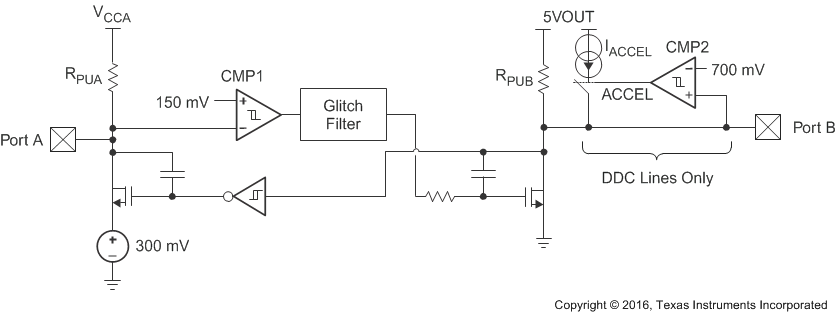
The TPD12S015A enables DDC translation from VCCA (system side) voltage levels to 5-V (HDMI cable side) voltage levels without degradation of system performance. The TPD12S015A contains two bidirectional open-drain buffers specifically designed to support up-translation and down-translation between the low voltage, VCCA side DDC-bus and the 5-V DDC-bus. The port B I/Os are overvoltage tolerant to 5.5 V even when the device is unpowered. After power up and with the LS_OE and CT_CP_HPD pins high, a low level on port A (below approximately VILC = 0.08 × VCCA V) turns the corresponding port B driver (either SDA or SCL) on and drives port B down to VOLB V. When port A rises above approximately 0.10 × VCCA V, the port B pulldown driver is turned off, and the internal pullup resistor pulls the pin high. When port B falls first and goes below 0.3 × 5VOUT, a CMOS hysteresis input buffer detects the falling edge, turns on the port A driver, and pulls port A down to approximately VOLA = 0.16 × VCCA V. The port B pulldown is not enabled unless the port A voltage goes below VILC. If the port A low voltage goes below VILC, the port B pulldown driver is enabled until port A rises above (VILC + ΔVT-HYSTA); then port B, if not externally driven LOW, continues to rise being pulled up by the internal pullup resistor.
 Figure 15. DDC/CEC Level Shifter Block Diagram
8.3.6 DDC/CEC Level Shifting Function When VCCA = 1.8 V
- The threshold of CMP1 is approximately 150 mV ± the 40 mV of total hysteresis.
- The comparator trips for a falling waveform at approximately 130 mV
- The comparator trips for a rising waveform at approximately 170 mV
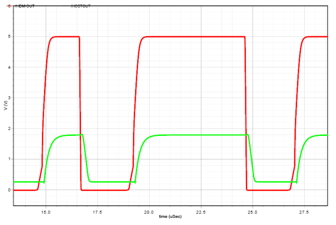
- To be recognized as a zero, the level at Port A must first go below 130 mV (VILC in spec) and then stay below 170 mV (VILA in spec)
- To be recognized as a one, the level at A must first go above 170 mV and then stay above 130 mV
- VILC is set to 110 mV to give some margin to the 130 mV
- VILA is set to 140 mV to give some margin to the 170 mV
- VIHA is set to 70% of VCCA to be consistent with standard CMOS levels
 Figure 16. DDC/CEC Level Shifter Operation (B to A Direction)
8.3.7 CEC Level Shifting Function
The CEC level shift function operates in the same manner as the DDC lines except that the CEC line does not need the rise time accelerator function.
8.4 Device Functional Modes
8.4.1 Enable
The DC-DC converter is enabled when the CT_CP_HPD is set to high. At first, the internal reference is activated and the internal analog circuits are settled. Afterwards, the soft start is activated and the output voltage is ramped up. The output voltage reaches its nominal value in typically 250 μs after the device has been enabled. The CT_CP_HPD input can be used to control power sequencing in a system with various DC-DC converters. The CT_CP_HPD pin can be connected to the output of another converter, to drive the EN pin high and getting a sequencing of supply rails. With CT_CP_HPD = GND, the DC-DC enters shutdown mode.
8.4.2 Power Save Mode
The TPD12S015A integrates a power save mode to improve efficiency at light load. In power save mode the converter only operates when the output voltage trips below a set threshold voltage. It ramps up the output voltage with several pulses and goes into power save mode once the output voltage exceeds the set threshold voltage. The PFM mode is left and PWM mode entered in case the output current can not longer be supported in PFM mode.
Table 2. System Block Diagram Function Table
| LS_OE | CT_CP_HPD | VCCA | VBAT | 5VOUT | A-SIDE | DDC, B-SIDE | CEC, B-SIDE | CEC LDO | DC-DC & HPD | DDC/CEC | ICC VCCA | ICC VBAT | COMMENT |
|---|---|---|---|---|---|---|---|---|---|---|---|---|---|
| PULLUPS | PULLUPS | PULLUPS | VLTs | TYP | TYP | ||||||||
| L | L | 1.8 V | 3.3 V | Off | Off | Off | Off | Off | Off | Off | 1 µA | 1 µA | Fully Disabled |
| L | H | 1.8 V | 3.3 V | On | On | On | Off | Off | On | Off | 1 µA | 30 µA | DC-DC on |
| H | L | 1.8 V | 3.3 V | Off | Off | Off | Off | Off | Off | Off | 1 µA | 1 µA | Not Valid State |
| H | H | 1.8 V | 3.3 V | On | On | On | On | On | On | On | 13 µA | 255 µA | Fully On |
| X | X | 0 V | 0 V | Off | High-Z | High-Z | High-Z | Off | Off | Off | 0 | 0 | Power Down |
| X | X | 1.8 V | 0 V | Off | Low | High-Z | High-Z | Off | Off | Off | 0 | 0 | Power Down |
| X | X | 0 V | 3.3 V | Off | High-Z | High-Z | High-Z | Off | Off | Off | 0 | 0 | Power Down |