SLLSEH9B October 2013 – July 2016 TPD1S414
PRODUCTION DATA.
- 1 Features
- 2 Applications
- 3 Description
- 4 Revision History
- 5 Pin Configuration and Functions
-
6 Specifications
- 6.1 Absolute Maximum Ratings
- 6.2 ESD Ratings
- 6.3 Recommended Operating Conditions
- 6.4 Thermal Information
- 6.5 Electrical Characteristics (EN, ACK Pins)
- 6.6 Electrical Characteristics (OVP Circuit)
- 6.7 Timing Requirements
- 6.8 Switching Characteristics (nFET)
- 6.9 Supply Current Consumption
- 6.10 Thermal Shutdown Feature
- 6.11 Typical Characteristics
-
7 Detailed Description
- 7.1 Overview
- 7.2 Functional Block Diagram
- 7.3
Feature Description
- 7.3.1 Overvoltage Protection on VBUS_CON up to 30-V DC
- 7.3.2 Low RON nFET Switch Supports Host and Charging Mode
- 7.3.3 ±15-kV IEC 61000-4-2 Level 4 ESD Protection
- 7.3.4 100-V IEC 61000-4-5 µs Surge Protection
- 7.3.5 Start-Up and OVP Recovery Delay
- 7.3.6 Integrated Input Enable and Status Output Signal
- 7.3.7 Thermal Shutdown
- 7.4 Device Functional Modes
- 8 Application and Implementation
- 9 Power Supply Recommendations
- 10Layout
- 11Device and Documentation Support
- 12Mechanical, Packaging, and Orderable Information
Package Options
Refer to the PDF data sheet for device specific package drawings
Mechanical Data (Package|Pins)
- YZ|12
Thermal pad, mechanical data (Package|Pins)
Orderable Information
5 Pin Configuration and Functions
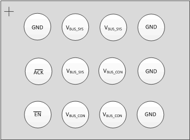
YZ Package
12-Pin DSBGA
Top View - See Through

Pin Functions
| PIN | TYPE | DESCRIPTION | |
|---|---|---|---|
| NAME | NO. | ||
| ACK | B1 | O | Open-Drain Acknowledge pin. See Table 2. |
| EN | C1 | I | Enable Active-Low Input. Drive EN low to enable the switch. Drive EN high to disable the switch. |
| VBUS_CON | B3, C2, C3 | I/O | Connect to USB connector VBUS pin; IEC61000-4-2 ESD protection IEC61000-4-5 Surge protection |
| VBUS_SYS | A2, A3, B2 | I/O | Connect to internal VBUS plane |
| GND | A1, A4, B4, C4 | Ground | Connect to PCB ground plane |
Table 1. 12-YZ Pin Mapping
| 1 | 2 | 3 | 4 | |
|---|---|---|---|---|
| A | GND | VBUS_SYS | VBUS_SYS | GND |
| B | ACK | VBUS_SYS | VBUS_CON | GND |
| C | EN | VBUS_CON | VBUS_CON | GND |