SLVSDG5C March 2016 – August 2020 TPD3S014-Q1
PRODUCTION DATA
- 1 Features
- 2 Applications
- 3 Description
- 4 Revision History
- 5 Pin Configuration and Functions
-
6 Specifications
- 6.1 Absolute Maximum Ratings
- 6.2 ESD Ratings—AEC Specification
- 6.3 ESD Ratings—IEC Specification
- 6.4 ESD Ratings—ISO Specification
- 6.5 Recommended Operating Conditions
- 6.6 Thermal Information
- 6.7 Electrical Characteristics: TJ = TA = 25°C
- 6.8 Electrical Characteristics: –40°C ≤ TA ≤ 105°C
- 6.9 Typical Characteristics
- 7 Parameter Measurement Information
- 8 Detailed Description
- 9 Application and Implementation
- 10Power Supply Recommendations
- 11Layout
- 12Device and Documentation Support
- 13Mechanical, Packaging, and Orderable Information
Package Options
Mechanical Data (Package|Pins)
- DBV|6
Thermal pad, mechanical data (Package|Pins)
Orderable Information
3 Description
The TPD3S014-Q1 is an integrated device that features a current-limited load switch and a two-channel transient voltage suppressor (TVS) based electrostatic discharge (ESD) protection diode array for USB interfaces.
The TPD3S014-Q1 device is intended for applications such as USB where heavy capacitive loads and short-circuits are likely to be encountered; the TPD3S014-Q1 provides short-circuit protection and overcurrent protection. The TPD3S014-Q1 limits the output current to a safe level by operating in constant current mode when the output load exceeds the current limit threshold. The fast overload response eases the burden on the main 5 V power supply by quickly regulating the power when the output is shorted. The rise and fall times for the current limit switch are controlled to minimize current surges when turning the device on and off.
The TPD3S014-Q1 allows 0.5 A of continuous current. The TVS diode array is rated to dissipate ESD strikes above the maximum level specified in the IEC 61000-4-2 international standard.
The high level of integration, combined with its easy-to-route DBV package, allows this device to provide great circuit protection for USB interfaces in applications like head units, USB hubs, and media interfaces.
| PART NUMBER | PACKAGE | BODY SIZE (NOM) |
|---|---|---|
| TPD3S014-Q1 | SOT-23 (6) | 2.90 mm × 1.60 mm |
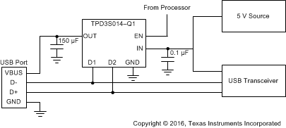
 Simplified Schematic