SLVSDG5C March 2016 – August 2020 TPD3S014-Q1
PRODUCTION DATA
- 1 Features
- 2 Applications
- 3 Description
- 4 Revision History
- 5 Pin Configuration and Functions
-
6 Specifications
- 6.1 Absolute Maximum Ratings
- 6.2 ESD Ratings—AEC Specification
- 6.3 ESD Ratings—IEC Specification
- 6.4 ESD Ratings—ISO Specification
- 6.5 Recommended Operating Conditions
- 6.6 Thermal Information
- 6.7 Electrical Characteristics: TJ = TA = 25°C
- 6.8 Electrical Characteristics: –40°C ≤ TA ≤ 105°C
- 6.9 Typical Characteristics
- 7 Parameter Measurement Information
- 8 Detailed Description
- 9 Application and Implementation
- 10Power Supply Recommendations
- 11Layout
- 12Device and Documentation Support
- 13Mechanical, Packaging, and Orderable Information
Package Options
Mechanical Data (Package|Pins)
- DBV|6
Thermal pad, mechanical data (Package|Pins)
Orderable Information
9.2.3 Implementing Active Low Logic
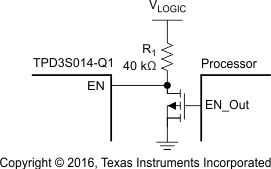
For active low logic, a transistor can be used with the TPD3S014-Q1 EN Pin. Figure 9-2 shows how to implement Active low logic for EN pin.
Using an nFET transistor, when the Processor sends a low signal, the transistor is switched off, and VLOGIC pulls up EN through R1. When the Processor sends a “high” signal, the nFET is switched on and sinks current from the EN Pin and R1. For 5 V VLOGIC, with the appropriate on-resistance (RON) value in the nFET and resistance for R1, the VIL for EN can be met. For example, with a transistor with RON of 3 Ω, a pull-up resistor as low as 11 Ω provides a logic level of 0.7 V. For power-budgeting concerns, a better choice is R1 of 40 kΩ which provides 0.25 V for EN when the Processor asserts high, and 4.96 V when the Processor asserts low.
 Figure 9-2 Implementing Active Low Logic for EN Pin