SLLSEG0F March 2013 – September 2017 TPD4E001-Q1
PRODUCTION DATA.
- 1 Features
- 2 Applications
- 3 Description
- 4 Revision History
- 5 Pin Configuration and Functions
- 6 Specifications
- 7 Detailed Description
- 8 Application and Implementation
- 9 Power Supply Recommendations
- 10Layout
- 11Device and Documentation Support
- 12Mechanical, Packaging, and Orderable Information
Package Options
Mechanical Data (Package|Pins)
- DBV|6
Thermal pad, mechanical data (Package|Pins)
Orderable Information
7 Detailed Description
7.1 Overview
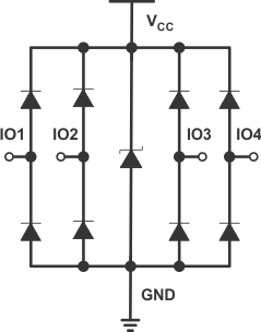
The TPD4E001-Q1 device is a low-capacitance, TVS diode array designed for ESD protection in sensitive electronics connected to communication lines. Each channel consists of a pair of transient voltage suppression diodes that steer ESD pulses to VCC or GND. The TPD4E001-Q1 device protects against ESD events up to ±8-kV contact discharge and ±15-kV air-gap discharge, as specified in IEC 61000-4-2 international standard. This device has a low capacitance of 1.5-pF per channel making it ideal for use in high-speed data interfaces. The low-leakage current (10 nA maximum) ensures minimum power consumption for the system and high accuracy for analog interfaces.
7.2 Functional Block Diagram

7.3 Feature Description
7.3.1 AEC-Q100 Qualified
This device is qualified according to the AEC-Q100 standard. The device temperature rating is Grade 1 (–40°C to +125°C). The HBM Classification Level passed is 3B (> 8 kV). The CDM Classification Level passed is C5 (all pins 750 V to <1000 V).
7.3.2 IEC 61000-4-2 Level 4 ESD Protection
The device is specified at ±8-kV contact discharge and ±15-kV air gap discharge.
7.3.3 IEC 61000-4-5 Surge Protection
This device is rated to pass at least 5.5-A of peak pulse current according to the IEC 61000-4-5 (8/20-µs pulse) standard.
7.3.4 Low 1.5-pF Input Capacitance
This device has a typical capacitance of 1.5-pF on each of the four IO pins. This allows for high speed signals on the IO pins in excess of 1 Gbps.
7.3.5 Low 10-nA (Maximum) Leakage Current
This device is rated to have a maximum leakage current of 10-nA on each of the four IO pins.
7.3.6 0.9-V to 5.5-V Supply Voltage Range
This device is specified to operate with a supply voltage (on VCC) between 0.9-V and 5.5-V to ensure sufficient signal integrity.
7.4 Device Functional Modes
The TPD4E001-Q1 device is a passive integrated circuit that triggers when voltages are above VBR or below the lower diodes VF (–0.6 V). During ESD events, voltages as high as ±8 kV (contact) can be directed to ground via the internal diode network. Once the voltages on the protected line fall below the trigger levels of TPD4E001-Q1 (usually within 10s of nano-seconds) the device reverts back to its high-impedance state.