SLLSEG0F
March 2013 – September 2017
TPD4E001-Q1
PRODUCTION DATA.
1
Features
2
Applications
3
Description
4
Revision History
5
Pin Configuration and Functions
6
Specifications
6.1
Absolute Maximum Ratings
6.2
ESD Ratings—AEC Specification
6.3
ESD Ratings—IEC Specification
6.4
ESD Ratings—ISO Specification
6.5
Recommended Operating Conditions
6.6
Thermal Information
6.7
Electrical Characteristics
6.8
Typical Characteristics
7
Detailed Description
7.1
Overview
7.2
Functional Block Diagram
7.3
Feature Description
7.3.1
AEC-Q100 Qualified
7.3.2
IEC 61000-4-2 Level 4 ESD Protection
7.3.3
IEC 61000-4-5 Surge Protection
7.3.4
Low 1.5-pF Input Capacitance
7.3.5
Low 10-nA (Maximum) Leakage Current
7.3.6
0.9-V to 5.5-V Supply Voltage Range
7.4
Device Functional Modes
8
Application and Implementation
8.1
Application Information
8.2
Typical Application
8.2.1
Design Requirements
8.2.2
Detailed Design Procedure
8.2.2.1
Signal Range on IO1 Through IO4
8.2.2.2
Voltage Range on VCC
8.2.2.3
Bandwidth on IO1 Through IO4
8.2.3
Application Curve
9
Power Supply Recommendations
10
Layout
10.1
Layout Guidelines
10.2
Layout Example
11
Device and Documentation Support
11.1
Documentation Support
11.1.1
Related Documentation
11.2
Receiving Notification of Documentation Updates
11.3
Community Resources
11.4
Trademarks
11.5
Electrostatic Discharge Caution
11.6
Glossary
12
Mechanical, Packaging, and Orderable Information
Package Options
Mechanical Data (Package|Pins)
DBV|6
MPDS026Q
Thermal pad, mechanical data (Package|Pins)
Orderable Information
sllseg0f_oa
sllseg0f_pm
5
Pin Configuration and Functions
DBV Package
6-Pin SOT-23
Top View
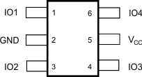
Pin Functions
PIN
TYPE
DESCRIPTION
NAME
NO.
GND
2
GND
Ground
IO1
1
I/O
ESD-protected channel
IO2
3
IO3
4
IO4
6
V
CC
5
I
Power-supply input. Bypass V
CC
to GND with a 0.1-μF ceramic capacitor