SLLS907E August 2008 – August 2014 TPD4F003 , TPD6F003 , TPD8F003
PRODUCTION DATA.
- 1 Features
- 2 Applications
- 3 Description
- 4 Revision History
- 5 Pin Configuration and Functions
- 6 Specifications
-
7 Detailed Description
- 7.1 Overview
- 7.2 Functional Block Diagram
- 7.3
Feature Description
- 7.3.1 Four-, Six-, and Eight-Channel EMI Filtering for Data Ports
- 7.3.2 -3 dB Bandwidth of 200 MHz
- 7.3.3 Greater Than 25 dB Attenuation at 1 GHz
- 7.3.4 Robust ESD Protection Exceeds IEC 61000-4-2
- 7.3.5 Pi-Style (C-R-C) Filter Configuration
- 7.3.6 Low 10-nA Leakage Current
- 7.3.7 Easy Flow-Through Routing
- 7.4 Device Functional Modes
- 8 Applications and Implementation
- 9 Power Supply Recommendations
- 10Layout
- 11Device and Documentation Support
- 12Mechanical, Packaging, and Orderable Information
Package Options
Refer to the PDF data sheet for device specific package drawings
Mechanical Data (Package|Pins)
- DQD|8
Thermal pad, mechanical data (Package|Pins)
- DQD|8
Orderable Information
7 Detailed Description
7.1 Overview
The TPDxF003 family is a series of highly integrated devices designed to provide EMI filtering in all systems subjected to electromagnetic interference. These filters also provide a Transient Voltage Suppressor (TVS) diode circuit for ESD protection which prevents damage to the application when subjected to ESD stress far exceeding IEC 61000-4-2 (Level 4).
7.2 Functional Block Diagram
7.3 Feature Description
The TPDxF003 family is a line of ESD and EMI filtering devices designed to reduce EMI emissions and provide system level ESD protection. Each device can dissipate ESD strikes above the maximum level specified by IEC 61000-4-2 international standard. Additionally, the EMI filtering structure reduces EMI emissions by providing high frequency roll-off.
7.3.1 Four-, Six-, and Eight-Channel EMI Filtering for Data Ports
These devices provide EMI filtering for four, six, or eight channels of data lines.
7.3.2 –3 dB Bandwidth of 200 MHz
These devices have a through –3dB bandwidth of 200 MHz.
7.3.3 Greater Than 25 dB Attenuation at 1 GHz
Signal attenuation is above 25dB at 1 GHz, which provides significant reduction in spurious emissions.
7.3.4 Robust ESD Protection Exceeds IEC 61000-4-2
The ESD protection on all pins exceeds the IEC 61000-4-2 level 4 standard. Contact ESD is rated at ±12 kV and Air-gap ESD is rated at ±20 kV.
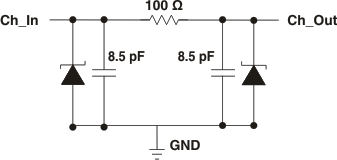
7.3.5 Pi-Style (C-R-C) Filter Configuration
This family of devices has a pi-style filtering configuration composed of a series resistor and two capacitors in parallel with the I/O pins. The typical resistor value is 100 Ω and the typical capacitor values are 8.5 pF each.
7.3.6 Low 10-nA Leakage Current
The I/O pins feature an ultra-low leakage current of 10-nA (typical) with a bias of 3.3 V.
7.3.7 Easy Flow-Through Routing
The layout of this device makes it easy to add protection to existing layouts. The packages offer flow-through routing which requires minimal changes to existing layout for addition of these devices.
7.4 Device Functional Modes
The TPDxF003 family of devices are passive integrated circuits that passively filter EMI and trigger when voltages are above VBR or below the lower diode voltage (–0.6 V). During ESD events, voltages as high as ±20 kV (air) can be directed to ground via the internal diode network. Once the voltages on the protected line fall below the trigger levels, the device reverts to passive.