SLLS907E August 2008 – August 2014 TPD4F003 , TPD6F003 , TPD8F003
PRODUCTION DATA.
- 1 Features
- 2 Applications
- 3 Description
- 4 Revision History
- 5 Pin Configuration and Functions
- 6 Specifications
-
7 Detailed Description
- 7.1 Overview
- 7.2 Functional Block Diagram
- 7.3
Feature Description
- 7.3.1 Four-, Six-, and Eight-Channel EMI Filtering for Data Ports
- 7.3.2 -3 dB Bandwidth of 200 MHz
- 7.3.3 Greater Than 25 dB Attenuation at 1 GHz
- 7.3.4 Robust ESD Protection Exceeds IEC 61000-4-2
- 7.3.5 Pi-Style (C-R-C) Filter Configuration
- 7.3.6 Low 10-nA Leakage Current
- 7.3.7 Easy Flow-Through Routing
- 7.4 Device Functional Modes
- 8 Applications and Implementation
- 9 Power Supply Recommendations
- 10Layout
- 11Device and Documentation Support
- 12Mechanical, Packaging, and Orderable Information
Package Options
Refer to the PDF data sheet for device specific package drawings
Mechanical Data (Package|Pins)
- DQD|8
Thermal pad, mechanical data (Package|Pins)
- DQD|8
Orderable Information
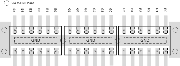
10 Layout
10.1 Layout Guidelines
- The optimum placement is as close to the connector as possible.
- EMI during an ESD event can couple from the trace being struck to other nearby unprotected traces, resulting in early system failures.
- The PCB designer needs to minimize the possibility of EMI coupling by keeping any unprotected traces away from the protected traces which are between the TVS and the connector.
- Route the protected traces as straight as possible.
- Eliminate any sharp corners on the protected traces between the TVS and the connector by using rounded corners with the largest radii possible.
- Electric fields tend to build up on corners, increasing EMI coupling.
10.2 Layout Example
This application is typical of an 18-bit RGB display panel layout.