SLLS907E August 2008 – August 2014 TPD4F003 , TPD6F003 , TPD8F003
PRODUCTION DATA.
- 1 Features
- 2 Applications
- 3 Description
- 4 Revision History
- 5 Pin Configuration and Functions
- 6 Specifications
-
7 Detailed Description
- 7.1 Overview
- 7.2 Functional Block Diagram
- 7.3
Feature Description
- 7.3.1 Four-, Six-, and Eight-Channel EMI Filtering for Data Ports
- 7.3.2 -3 dB Bandwidth of 200 MHz
- 7.3.3 Greater Than 25 dB Attenuation at 1 GHz
- 7.3.4 Robust ESD Protection Exceeds IEC 61000-4-2
- 7.3.5 Pi-Style (C-R-C) Filter Configuration
- 7.3.6 Low 10-nA Leakage Current
- 7.3.7 Easy Flow-Through Routing
- 7.4 Device Functional Modes
- 8 Applications and Implementation
- 9 Power Supply Recommendations
- 10Layout
- 11Device and Documentation Support
- 12Mechanical, Packaging, and Orderable Information
Package Options
Refer to the PDF data sheet for device specific package drawings
Mechanical Data (Package|Pins)
- DQD|12
Thermal pad, mechanical data (Package|Pins)
- DQD|12
Orderable Information
6 Specifications
6.1 Absolute Maximum Ratings(1)
over operating free-air temperature range (unless otherwise noted)| MIN | MAX | UNIT | |||
|---|---|---|---|---|---|
| VIO | IO to GND | 6 | V | ||
| TJ | Junction temperature | 150 | °C | ||
(1) Stresses beyond those listed under Absolute Maximum Ratings may cause permanent damage to the device. These are stress ratings only, and functional operation of the device at these or any other conditions beyond those indicated in the operational sections of the specifications is not implied. Exposure to absolute maximum rated conditions for extended periods may affect device reliability.
6.2 Handling Ratings
| MIN | MAX | UNIT | |||
|---|---|---|---|---|---|
| Tstg | Storage temperature range | –65 | 150 | °C | |
| V(ESD) | Electrostatic discharge | Human body model (HBM), per ANSI/ESDA/JEDEC JS-001, all pins(1) | ±15 | kV | |
| Charged device model (CDM), per JEDEC specification JESD22-C101, all pins(2) | ±1500 | V | |||
| IEC 61000-4-2 ESD Rating - Contact | ±12 | kV | |||
| IEC 61000-4-2 ESD Rating - Air | ±20 | ||||
(1) JEDEC document JEP155 states that 500-V HBM allows safe manufacturing with a standard ESD control process.
(2) JEDEC document JEP157 states that 250-V CDM allows safe manufacturing with a standard ESD control process.
6.3 Recommended Operating Conditions
over operating free-air temperature range (unless otherwise noted)| MIN | MAX | UNIT | ||
|---|---|---|---|---|
| VIO | 0 | 5.5 | V | |
| TA | –40 | 85 | °C | |
6.4 Thermal Information
| THERMAL METRIC(1) | TPD4F003 | TPD6F003 | TPD8F003 | UNIT | |
|---|---|---|---|---|---|
| DQD | |||||
| 8 PINS | 12 PINS | 16 PINS | |||
| RθJA | Junction-to-ambient thermal resistance | 115.6 | 89.2 | 80.8 | °C/W |
| RθJC(top) | Junction-to-case (top) thermal resistance | 108.5 | 100.1 | 88.3 | |
| RθJB | Junction-to-board thermal resistance | 66.4 | 50.5 | 45.8 | |
| ψJT | Junction-to-top characterization parameter | 6.8 | 9.4 | 9.2 | |
| ψJB | Junction-to-board characterization parameter | 65.9 | 50.0 | 45.4 | |
| RθJC(bot) | Junction-to-case (bottom) thermal resistance | 33.2 | 31.0 | 31.8 | |
(1) For more information about traditional and new thermal metrics, see the IC Package Thermal Metrics application report, SPRA953.
6.5 Electrical Characteristics
TA = –40°C to 85°C (unless otherwise noted)| PARAMETER | TEST CONDITIONS | MIN | TYP(1) | MAX | UNIT | |
|---|---|---|---|---|---|---|
| VBR | DC breakdown voltage | IIO = 10 μA | 6 | V | ||
| R | Resistance | 85 | 100 | 115 | Ω | |
| C | Capacitance (C1 or C2) | VIO = 2.5 V | 8.5 | pF | ||
| IIO | Channel leakage current | VIO = 3.3 V | 10 | nA | ||
| fC | Cut-off frequency | ZSOURCE = 50 Ω, ZLOAD = 50 Ω | 200 | MHz | ||
(1) Typical values are at TA = 25°C.
6.6 Typical Characteristics
6.6.1 IEC Clamping Waveforms
(clamp voltage measured both at Ch_Out and Ch_In)
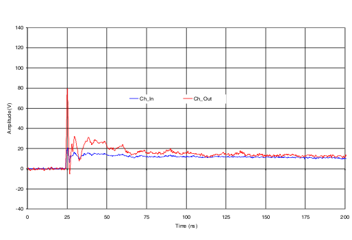 Figure 1. With 8 kV Contact ESD Stress at Ch_Out
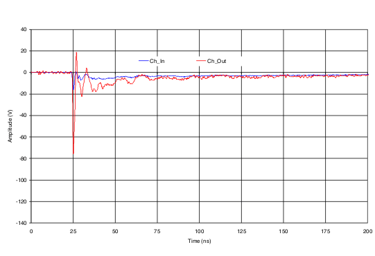 Figure 3. With -8 kV Contact ESD Stress at Ch_Out
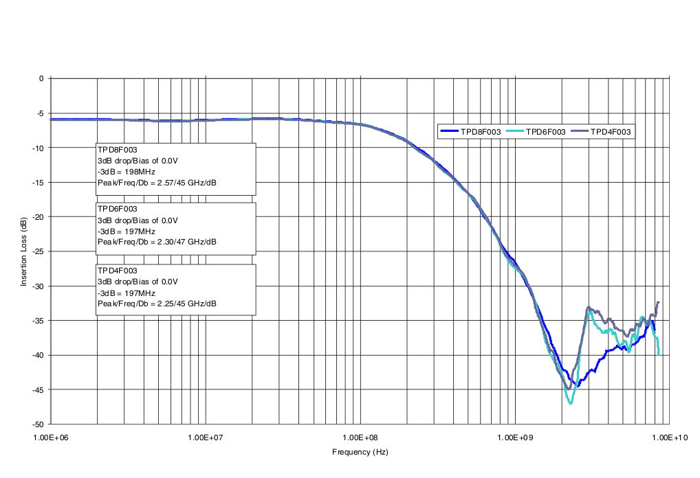
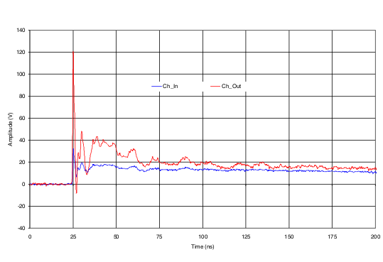 Figure 2. With 12 kV Contact ESD Stress at Ch_Out
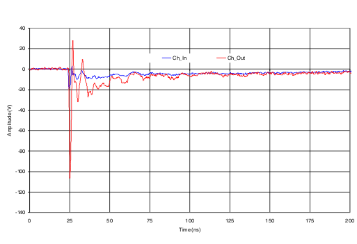 Figure 4. With -12 kV Contact ESD Stress at Ch_Out
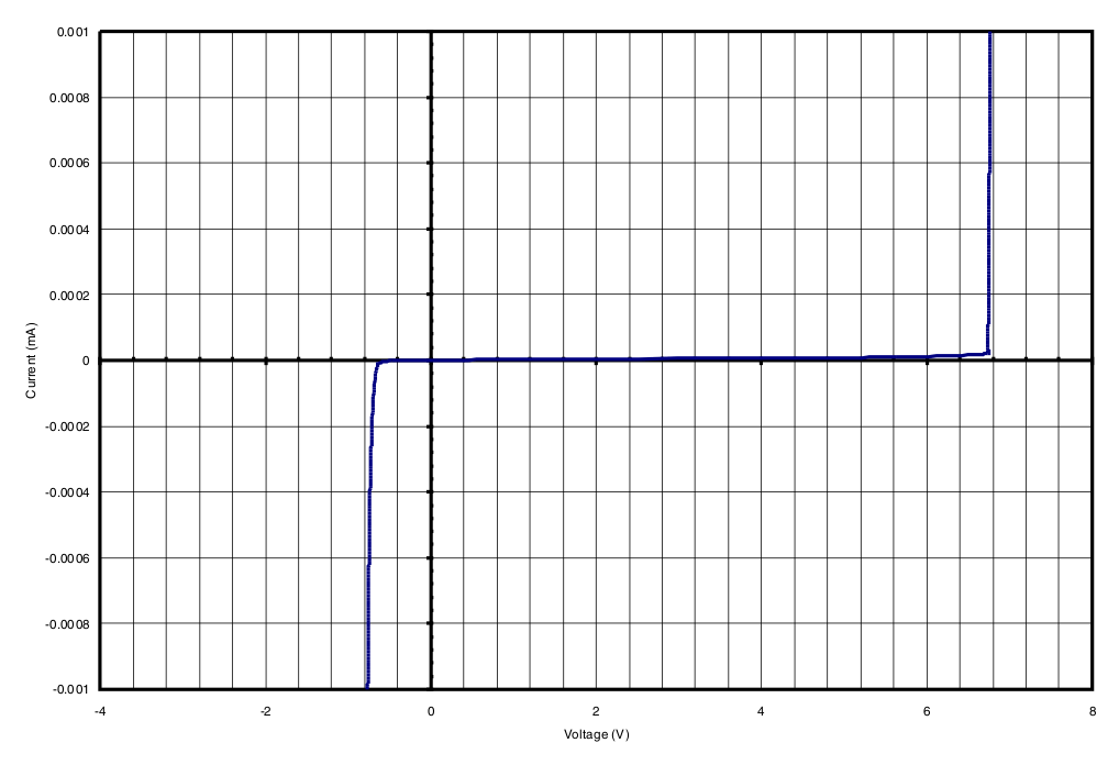 Figure 6. DC Voltage-Current Sweep Across Input/Output Pins
6.6.2 Channel-to-Channel Crosstalk
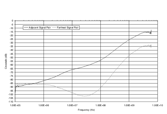 Figure 7. TPD4F003
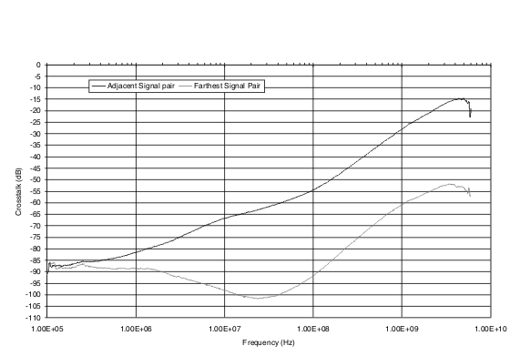 Figure 9. TPD8F003
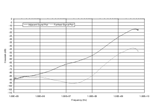 Figure 8. TPD6F003