SLLSE33E August 2010 – December 2016 TPD7S019
PRODUCTION DATA.
- 1 Features
- 2 Applications
- 3 Description
- 4 Revision History
- 5 Pin Configuration and Functions
- 6 Specifications
- 7 Detailed Description
- 8 Application and Implementation
- 9 Power Supply Recommendations
- 10Layout
- 11Device and Documentation Support
- 12Mechanical, Packaging, and Orderable Information
Package Options
Mechanical Data (Package|Pins)
Thermal pad, mechanical data (Package|Pins)
- RSV|16
Orderable Information
7 Detailed Description
7.1 Overview
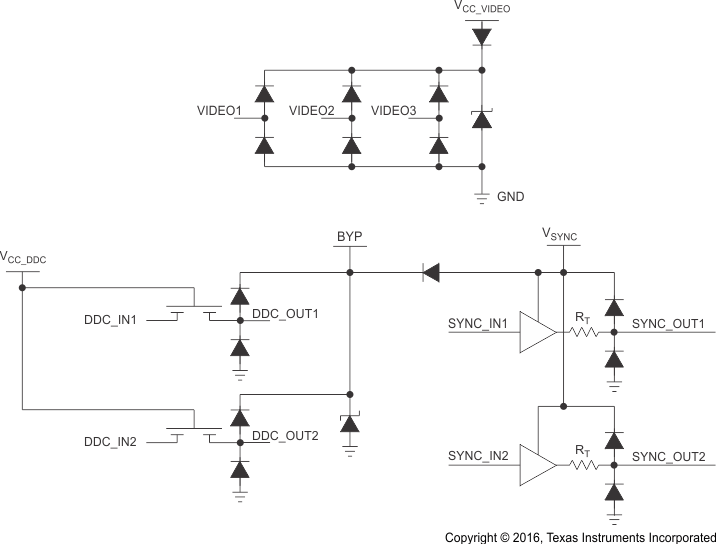
The TPD7S019 is an integrated protection solution for VGA or DVI-I ports by providing high-speed ESD protection, level-shifting and signal buffering. The TVS protection diodes for VIDEO signals, DDC signals and SYNC signals provide robust ESD clamping that meets the IEC61000-4-2 standard for ±8-kV contact stress. The signals run at high speed is minimally affected by the low capacitance added to each signal line. The integrated level-shifters for the DDC signals help save external ICs. Two buffers on the HSYNC and VSYNC signals convert TTL input level to CMOS output level, and it saves external components by integrating series termination resistors connected to the SYNC_OUT pin. The TPD7S019 takes in three signal rails to make the signals compatible with different voltages on VIDEO, DDC and SYNC. The two package options provide the latitude to choose between either small board area or easier layout and better signal integrity.
The end applications of this device include desktop and laptop PCs, set top boxes, TVs, and monitors.
7.3 Feature Description
The TPD7S019 is an integrated protection solution for VGA and DVI-I ports. It has the low capacitance ESD TVS diodes for the VIDEO signals to ensure high speed data transmission. Level-shifting on the DDC lines translate signals on the cable to the level can be processed by downstream ICs. Buffers on the SYNC lines condition the signal levels and quality. The integrated termination resistors help reduce external devices. The TPD7S019 exceeds IEC61000-4-2 (Level 4) ESD standard of ±8-kV contact discharge, making the system robust against system level ESD. The two package options provide the freedom to choose between a compact package or a flow through package.
7.4 Device Functional Modes
DDC level translators and SYNC signal buffers are active and the ESD cells on all the lines are untriggered when the recommended operating conditions are met. The bidirectional voltage-level translators provide noninverting level-shifting from the system side to the connector side. Each connector side pin has an ESD clamp that triggers when voltages are above VBR or below the lower diode's Vf. During ESD events, voltages as high as ±8-kV (contact ESD) can be directed to ground through the internal diode network. Once the voltages on the protected line fall below these trigger levels (usually within 10s of nano-seconds), these pins revert to a non-conductive state.
