SLLSE33E August 2010 – December 2016 TPD7S019
PRODUCTION DATA.
- 1 Features
- 2 Applications
- 3 Description
- 4 Revision History
- 5 Pin Configuration and Functions
- 6 Specifications
- 7 Detailed Description
- 8 Application and Implementation
- 9 Power Supply Recommendations
- 10Layout
- 11Device and Documentation Support
- 12Mechanical, Packaging, and Orderable Information
Package Options
Mechanical Data (Package|Pins)
Thermal pad, mechanical data (Package|Pins)
- RSV|16
Orderable Information
10 Layout
10.1 Layout Guidelines
The optimum placement of this device is as close to the connector as possible. EMI during an ESD event can couple from the trace being struck to other nearby unprotected traces, resulting in early system failures. Therefore, the PCB designer needs to minimize the possibility of EMI coupling by keeping any unprotected traces away from the protected traces which are between the TVS and the connector.
Route the protected traces as straight as possible.
Avoid using VIAs between the connecter and an I/O protection pin on the TPD7S019.
Avoid 90º turns in traces since electric fields tend to build up on corners, increasing EMI coupling.
Minimize impedance on the path to GND for maximum ESD dissipation.
The capacitors on VCC_VIDEO, VCC_DDC and VCC_SYNC must be placed close to their respective pins.
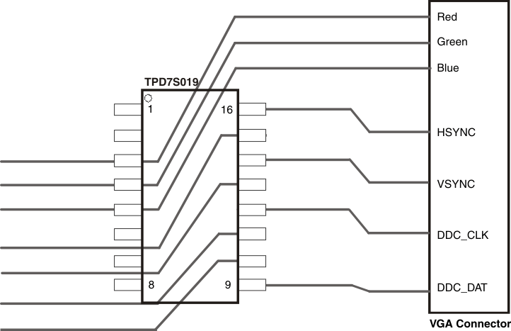
The VIDEO lines internal protection circuits are the same and thus these pins are interchangeable for routing.
10.2 Layout Example
 Figure 9. Simplified Layout with TPD7S019 (Only IO Lines are Shown)