SLLSE33E August 2010 – December 2016 TPD7S019
PRODUCTION DATA.
- 1 Features
- 2 Applications
- 3 Description
- 4 Revision History
- 5 Pin Configuration and Functions
- 6 Specifications
- 7 Detailed Description
- 8 Application and Implementation
- 9 Power Supply Recommendations
- 10Layout
- 11Device and Documentation Support
- 12Mechanical, Packaging, and Orderable Information
Package Options
Mechanical Data (Package|Pins)
Thermal pad, mechanical data (Package|Pins)
- RSV|16
Orderable Information
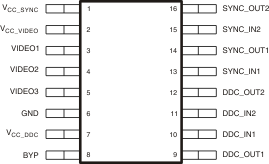
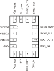
5 Pin Configuration and Functions
DBQ Package
16-Pin SSOP
Top View

Pin Functions
| PIN | TYPE | DESCRIPTION | ||
|---|---|---|---|---|
| NAME | DBQ | RSV | ||
| BYP | 8 | 6 | Power | Bypass pin. Using a 0.2-µF bypass capacitor increases the ESD robustness of the system |
| DDC_IN1 | 10 | 8 | I | DDC signal input. Connects to the VGA controller side of one of the sync lines |
| DDC_IN2 | 11 | 9 | ||
| DDC_OUT1 | 9 | 7 | O | DDC signal output. Connects to the video connector side of one of the sync lines |
| DDC_OUT2 | 12 | 10 | ||
| GND | 6 | 4 | — | Ground |
| SYNC_IN1 | 13 | 11 | I | Sync signal buffer input. Connects to the VGA controller side of one of the sync lines |
| SYNC_IN2 | 15 | 13 | ||
| SYNC_OUT1 | 14 | 12 | O | Sync signal buffer output. Connects to the video connector side of one of the sync lines |
| SYNC_OUT2 | 16 | 14 | ||
| VCC_DDC | 7 | 5 | Power | Isolated supply input for the DDC_1 and DDC_2 level-shifting N-FET gates |
| VCC_SYNC | 1 | 15 | Power | Isolated supply input for the SYNC_1 and SYNC_2 level-shifters and their associated ESD protection circuits |
| VCC_VIDEO | 2 | 16 | Power | Supply pin specifically for the VIDEO_1, VIDEO_2 and VIDEO_3 ESD protection circuits |
| VIDEO1 | 3 | 1 | ESD | High-speed ESD clamp input |
| VIDEO2 | 4 | 2 | ||
| VIDEO3 | 5 | 3 | ||
