SLIS171 December 2015 TPIC2030
PRODUCTION DATA.
- 1 Features
- 2 Applications
- 3 Description
- 4 Revision History
- 5 Description (continued)
- 6 Pin Configuration and Functions
-
7 Specifications
- 7.1 Absolute Maximum Ratings
- 7.2 ESD Ratings
- 7.3 Recommended Operating Conditions
- 7.4 Thermal Information
- 7.5 Electrical Characteristics - Common Part
- 7.6 Electrical Characteristics - Charge Pump Part
- 7.7 Electrical Characteristics - DC-DC Converter
- 7.8 Electrical Characteristics - Spindle Motor Driver Part
- 7.9 Electrical Characteristics - Sled Motor Driver Part
- 7.10 Electrical Characteristics - Focus/ Tilt/Tracking/Driver Part
- 7.11 Electrical Characteristics - Load Driver Part
- 7.12 Electrical Characteristics - Current Switch Part
- 7.13 Electrical Characteristics - LED Switch Part
- 7.14 Electrical Characteristics - Thermometer Part
- 7.15 Electrical Characteristics - Actuator Protection
- 7.16 Electrical Characteristics - Serial Port Voltage Levels
- 7.17 Serial Port I/F Write Timing Requirements
- 7.18 Serial I/F Read Timing Requirements
- 7.19 Typical Characteristics
-
8 Detailed Description
- 8.1 Overview
- 8.2 Functional Block Diagram
- 8.3 Feature Description
- 8.4 Device Functional Modes
- 8.5 Programming
- 8.6
Register Maps
- 8.6.1 Register State Transition
- 8.6.2 DAC Register (12-Bit Write Only)
- 8.6.3 Control Register
- 8.6.4
Detailed Description of Registers
- 8.6.4.1 REG01 12-bit DAC for Tilt (VDAC_MAPSW = 0)
- 8.6.4.2 REG02 12-bit DAC for Focus (VDAC_MAPSW = 0)
- 8.6.4.3 REG03 12-bit DAC for Track (VDAC_MAPSW = 0)
- 8.6.4.4 REG04 10bit DAC for Sled1 (VDAC_MAPSW = 0)
- 8.6.4.5 REG05 10bit DAC for Sled2 (VDAC_MAPSW = 0)
- 8.6.4.6 REG08 12-bit DAC for Spindle (VDAC_MAPSW = 0)
- 8.6.4.7 REG09 12-bit DAC for Load (VDAC_MAPSW = 0)
- 8.6.4.8 REG65 8bit Control Register for FBSVR
- 8.6.4.9 REG6D 8bit Control Register for DCCfg
- 8.6.4.10 REG6E 8bit Control Register for UtilCfg
- 8.6.4.11 REG6F 8bit Control Register for MonitorSet (REG6F)
- 8.6.4.12 REG70 8bit Control Register for DriverEna
- 8.6.4.13 REG71 8bit Control Register for FuncEna
- 8.6.4.14 REG72 8bit Control Register for ACTCfg
- 8.6.4.15 REG73 8bit Control Register for Parm0
- 8.6.4.16 REG74 8bit Control Register for OptSet
- 8.6.4.17 REG76 8bit Control Register for WriteEna
- 8.6.4.18 REG77 8bit Control Register for ClrReg
- 8.6.4.19 REG78 8bit Control Register for ActTemp
- 8.6.4.20 REG79 8bit Control Register for UVLOMon
- 8.6.4.21 REG7A 8bit Control Register for TsdMon
- 8.6.4.22 REG7B 8bit Control Register for ProtMon
- 8.6.4.23 REG7C 8bit Control Register for TempMon
- 8.6.4.24 REG7E 8bit Control Register for Version
- 8.6.4.25 REG7F 8bit Control Register for Status
-
9 Application and Implementation
- 9.1
Application Information
- 9.1.1 DAC Type
- 9.1.2 Example Sampling Rate of 12-Bit DAC for FCS/TRK/TLT
- 9.1.3 Digital Input Coding
- 9.1.4 Example Timing of Target Control System
- 9.1.5 Spindle Motor Driver Part
- 9.1.6 Sled Driver Part
- 9.1.7 Load Driver Part
- 9.1.8 Focus/Track/Tilt Driver Part
- 9.1.9 Step-Down Synchronous DC-DC Converter
- 9.1.10 Monitor Signal on GPOUT
- 9.2 Typical Application
- 9.1
Application Information
- 10Power Supply Recommendations
- 11Layout
- 12Device and Documentation Support
- 13Mechanical, Packaging, and Orderable Information
Package Options
Mechanical Data (Package|Pins)
- DBT|44
Thermal pad, mechanical data (Package|Pins)
Orderable Information
9 Application and Implementation
NOTE
Information in the following applications sections is not part of the TI component specification, and TI does not warrant its accuracy or completeness. TI’s customers are responsible for determining suitability of components for their purposes. Customers should validate and test their design implementation to confirm system functionality.
NOTE
- Operate every driver channel after 5-V power supplied and stable.
- Appropriate capacity of de-coupling capacitor is required enough value of over 10μF due to reduce influence of PWM switching noise. And the P5V pin needs to connect a filter of 1μF. It is effective to put bypass capacitor(about 0.1uF) near Power pin(P5V_1,P5V_2, P5V_SW,P5V_SPM)for PWM switching noise reduction on power and GND line.
- Much current flow to driver circuits, to consider as below matters.
- Pattern-lay-out and line-impedance. And noise influence from supply line.
9.1 Application Information
9.1.1 DAC Type
TPIC2030 has nine channels of Actuator. Each channel is assigned to the most suitable DAC engine with a different type respectively. ACT(F/T/Ti) has 12-bit DAC. Upper 8 (MSB sign bit) are converted at a time in 5 MHz and LSB 4 bits are output in sequence with 1.25-MHz PWM. SPIN, SLED, and Load DAC has same DAC types and sampling rate with 312 kHz. All channels except SLED have x6 gain. Table 33 shows configuration of each actuator.
Table 33. DAC Type
| FCS/TRK/TLT | SLED | SPIN | LOAD | |
|---|---|---|---|---|
| Resolution | 12 bit | 10 bit | 12 bit | 12 bit |
| Type | 8-bit oversampling | 10-bit voltage | 8-bit oversampling | 8-bit oversampling |
| Sampling | 1.25M / 10bit 312K / 12bit |
312K | 312K | |
| PWM frequency | 312 kHz | About 156 kHz(variable) | 156 kHz | 312 kHz |
| Out range | ±6 V | ±440 mA | ±6 V | ±6 V |
| Feedback | Voltage feedback | Current feedback | Power supply compensation | Voltage feedback Shared with TRK |
9.1.2 Example Sampling Rate of 12-Bit DAC for FCS/TRK/TLT
The input data is separated in the upper 8 bits and the lower 4 bits. Upper 8 bits (MSB sign 1 bit) will be put into 8bit current DAC in every 5 MHz. The lower 4bits will be put into one bit current DAC in sequence from upper to lower bit. This one-bit DAC output with PWM in 1.25 MHz. At any PWM duty, 100%, 75%, 50%, 25%, or 0%, will be summed in 8-bit current DAC in every 1.25 MHz. Thus, it takes 3.2 µs for all lower 4bits summing to PWM output. As a result, 12 bit data is sampled in every PWM cycle. Example of sampling rate for FCS/TRK/TLT is Figure 47.
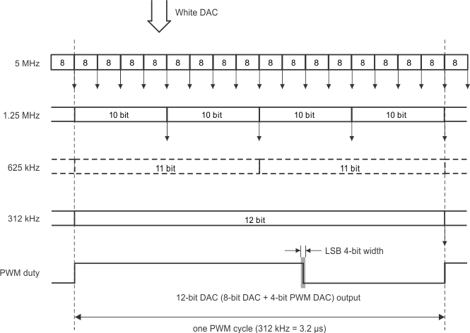 Figure 47. Example of 12-Bit DAC Conversion Time (FCS/TRK/TLT)
9.1.3 Digital Input Coding
The output voltage (current) is commanded via programming to the DAC. All of the DAC input format is 12bit in 2’s complement though some DAC has a low resolution. When 12 bits data is input 8 bits DAC, TPIC2030 recognizes four subordinate position bits (LSB) as 0. To arrange for 12-bit DAC format, DSP should shift 8bit or 10 bit data to an appropriate bit position. The full scale is ±1.0 V and driver gain is set 6. The output voltage (Vout) is given by the following equation:


where
- bit[11:0] is the digital input value, range 000000000000b to 111111111111b.
Table 34. DAC Format
| MSB DIGITAL INPUT (BIN) LSB | HEX | DEC | VDAC | ANALOG OUTPUT |
|---|---|---|---|---|
| 1000_0000_0000 | 0x800 | –2048 | –0.9995 | –5.997 |
| 1000_0000_0001 | 0x801 | –2047 | –0.9995 | –5.997 |
| 1111_1111_1111 | 0xFFF | –1 | –0.0005 | –0.003 |
| 0000_0000_0000 | 0x000 | 0 | 0 | 0.000 |
| 0000_0000_0001 | 0x001 | +1 | +0.0005 | +0.003 |
| 0111_1111_1110 | 0x7FE | +2046 | +0.9990 | +5.994 |
| 0111_1111_1111 | 0x7FF | +2047 | +0.9995 | +5.997 |
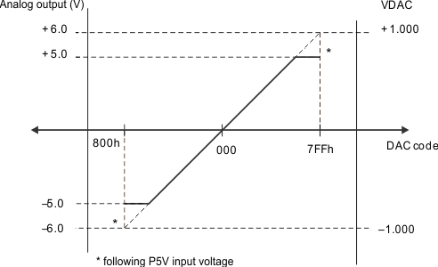 Figure 48. Output Voltage vs DAC Code
9.1.4 Example Timing of Target Control System
TPIC2030 is designed for that meets the requirements updating control data in 400 kHz. The example of control system parameter is listed in . It takes 0.51 µs for transmit a 16-bit data packet to TPIC2030 with 35 MHz SCLK. Therefore, DSP can be sent four packets a 400-kHz interval. If SCLK is lower than 28.8 MHz, it is required reducing packet quantity under three. For example, Focus/Track command is updating in every 2.5 µs (400 kHz), and it is able to send another two kind of packet in this same slot. shows the example of the control timing when TPIC2030 is used.
Table 35. Example Timing of Target Control System
| SIGNAL | BIT | UPDATE CYCLE (kHz) |
|---|---|---|
| Focus | 12 | 400 |
| Track | 12 | 400 |
| Tilt | 12 | 200 |
| Sled1 | 10 | 100 |
| Sled2 | 10 | 100 |
| Spindle | 12 | 100 |
| Load | 12 | — |
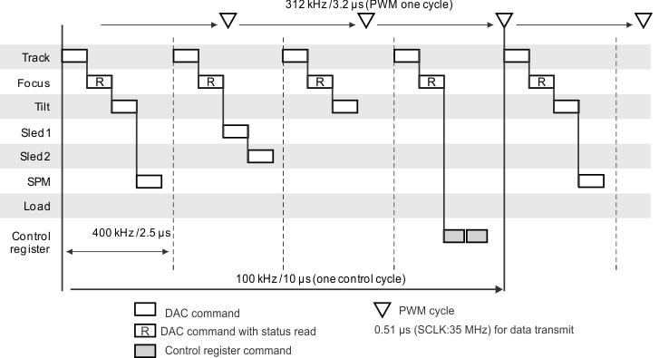 Figure 49. Example DAC Control
9.1.5 Spindle Motor Driver Part
When VSPM is set to a positive DAC code then the part will be in acceleration mode. IS mode operates then the start-up circuit offers the special start-up pattern sequence to the driver in start-up, and then switches to spin-up mode by detecting the rotor position by BEMF signal from the spindle motor coil.
The spin-down and brake function also be controlled by VSPM DAC value. When it is set the brake command to VSPM, driver goes into active-brake mode, then switch to short-brake mode in slow revolution speed, and then stop automatically. The FG signal is composed from EXOR of three-phase signal, and is output from XFG pin shown in Figure 50.
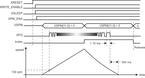 Figure 50. Spindle Operating Sequence
- It is recommended to use down-edge of FG signal for monitoring FG frequency. The FG terminal needs to be pull up to the appropriate supply voltage by external resistor.
- Short Brake mode is asserted after 300 ms of FG signal stays L-level in deceleration.
- The FG output is set to H-level in sleep mode in order to reduce sleep mode current.
- This value is the nominal number of using motor with 16-poles.
- First of all, power supply voltage of P5V must be supplied before any signals input.
9.1.5.1 Spindle PWM Control
The output PWM duty of Spindle is controlled by DAC code (VSPM). The gain in acceleration setting is always six times. However, the maximum output is restricted to P5V_SPM voltage. A dead band which output = 0 exists in the width of plus or minus 0x52 focusing on zero.
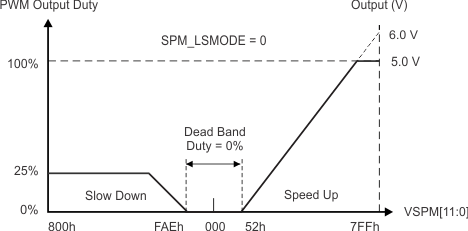 Figure 51. Spindle PWM Control
9.1.5.2 Auto Short Brake Function
TPIC2030 provides auto short brake function which is selecting brake mode automatically by motor speed.
Auto Short Brake is the intelligent brake function that includes 2 modes, Short Brake and Active Brake.
When VSPM value is controlled more than equivalent 75% duty brake, deceleration is done by short brake under the rotation speed is over 3000 rpm. After deceleration, driver goes into Active-brake mode automatically by internal logic circuit under rotation speed is lower 2000 rpm. This function enables low power consumption and silent during braking.
Table 36. Brake Mode
| VSPM[11:0] | ROTATION SPEED(RPM) | |
|---|---|---|
| ABOUT 0 TO 2000 | ABOUT 3000 | |
| 0x000 - 0xFAE | 2-phase short Brake | 2-phase short Brake |
| 0xFAE - 0xA00 | Active Brake | Active Brake |
| 0xA00 - 0x800 | Active Brake | 3-phase short Brake |
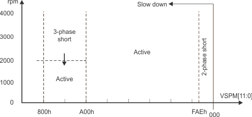 Figure 52. Brake Mode Selections
This value is the nominal number of using motor with 16-poles motor.
9.1.5.3 Spindle Low Speed Mode
LS mode is the low rotation mode which made the maximum 25% duty. When using SPM_LSMODE = 1, brake mode is always SHORT BRAKE. shows the output duty of LS mode.
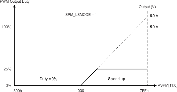 Figure 53. Spindle PWM Control (Low Speed Mode)
9.1.5.4 Spindle Driver Current Limit Circuit
This IC builds in the SPM current sense resistor which can select resistor value. .
The spindle current limit circuit monitors motor current which flows through this resistance, and limits the output current by reducing PWM duty when detecting over current conditions. shows resistor value.
A limit current value can be calculated from following formulas.
Limit current = 196mV / resistor value
Table 37. SPM Current Sense Resistor
| SPM_RCOM_SEL[1:0] | RESISTOR VALUE (Ω) | LIMIT CURRENT (mA) |
|---|---|---|
| 00 | 0.22 | 890 |
| 01 | 0.20 | 980 |
| 10 | 0.27 | 725 |
| 11 | 0.25 | 784 |
9.1.6 Sled Driver Part
9.1.6.1 Sled Channel Input vs Output PWM Duty
The Sled driver outputs the PWM pulse set as DAC code (VSLDx) with current feed back. The maximum output is restricted to 440mA at 0x7FF and 0x800. A dead band which output = 0 exists in the width of plus or minus focusing on zero.
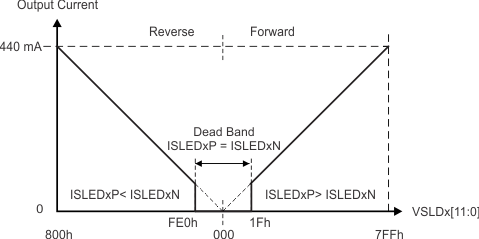 Figure 54. Sled Output Current
- Both outputs of SLED1/2 are L when input code is in dead band.
9.1.6.2 Sled End Detect Function
This device has the function of end position detection for Sled. By this function aim to eliminate the position switch at PUH inner. When this function is enabled, internal logic will detect the sled out zero-cross point and at that time, internal BEMF detect circuit measures the BEMF level of stepping motor. There’re four threshold levels. If BEMF is lower than selected threshold, device recognizes motor at stop and ENDDET bit to 1. ENDDET bit will be cleared at the BEMF voltage exceed threshold again.
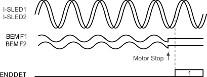 Figure 55. Timing of Sled End Detection
- In order to perform high-precision detection, the sled motor needs to generate higher BEMF voltage. BEMF level depends on the stepping motor characteristic and its speed.
- BEMF detection level is selectable 22, 46, 86 mV.
9.1.7 Load Driver Part
9.1.7.1 Load Channel Input vs Output PWM Duty
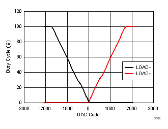
Load driver outputs the voltage with voltage feed back corresponding to the input DAC value. This channel has power voltage compensation thus it is suit for Slot-in type load control. This channel becomes active exclusively to other actuator channels. Load driver is shared with the TRK driver.
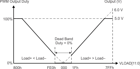 Figure 56. Load Output Duty
- Output voltage is controlled by PWM
- Both LOAD+ and LOAD- are connected to PGND through the internal clamp diode respectively.
9.1.8 Focus/Track/Tilt Driver Part
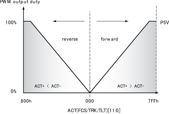 Figure 57. FCS/TRK/TLT Output Duty
9.1.8.1 Differential Tilt Mode
TPIC2030 support differential Tilt mode which output the value calculated from Focus and Tilt. Focus and Tilt can be set in differential mode by DIFF_TLT (REG74) = 1. Because Focus and Tilt are updated at the same time, the update interval of Tilt can be thinned out. Output data changes at after writing VFCS data. Therefore it is necessary to write VFCS data when set VTLT. In differential mode, the output value is calculated as follows.
9.1.9 Step-Down Synchronous DC-DC Converter
TPIC2030 has a synchronous step-down DC-DC converter which can output various voltages. Switching frequency is 2.5MHz. Because the ripple current in the coil can reduce, the smaller inductor value can be selected. And the inductor with lowest DC resistance can be selected for highest efficiency. And the regulators have fast transient response.
Step-down DC-DC converter produces an output 1.0, 1.2, 1.5, and 3.3 V. It only requires an external inductor and bypass capacitor(s). The gate drivers and compensations are all internal to the chip. The required input supply is 5 V for P5V_SW. It has a soft start approximately about 0.8 ms to limit the in-rush current when the regulator comes alive. The soft-start circuit uses the internal clock to profile its ramp.
It’s able to up 2%, 3.8% and 5.4% of the output voltage by setting SWR_VOUTUP (REG6D) for 1.2 V and 1.5 V, up 1.3%, 2.4%, and 3.3% for 1.0V.
Table 38. Output Voltage Setting
| SWR_VSEL2 | SWR_VSEL1 | INPUT REGFB | DCDC CONVERTER OUTPUT |
|---|---|---|---|
| 0 | 0 | <3.7 V | 3.3 V |
| 0 | 1 | <3.7 V | 1.2 V |
| 1 | 0 | <3.7 V | 1.0 V |
| 1 | 1 | <3.7 V | 1.5 V |
| X | X | over 3.7V | Disable (1) |
9.1.9.1 Discontinuous Regulation Mode
Provide a regulation mode named discontinuous regulation mode, which improves the conversion efficiency at a low current loading by changing regulation timing. Discontinuous mode is able to set 1 to SWR_MD_BURST (REG6D) bit. Furthermore by setting SWR_BSTAUTON (REG6D), the discontinuous mode is automatically chosen at the time of low power consumption. shows the discontinuous regulation action. The current consumption has been reduced by shortening the energizing time of driving FET. On the other hand, DC voltage ripple grows.
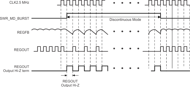 Figure 58. Discontinuous Regulation Mode
9.1.9.2 High Efficiency Mode (in Discontinuous Regulation Mode)
The high efficiency mode which raises efficiency further at the time of low consumption can be chosen for 1.0 V, 1.2 V, and 1.5 V. This mode is selected by SWR_BST_HEFF = 1 (REG6D) in discontinuous mode.
9.1.10 Monitor Signal on GPOUT
The device can output a specific signal to the GPOUT pin. To output a signal, choose a signal from REG6F by enabling first, then enable GPOUT_ENA. When two or more signals are set for GPOUT, the output is a logical sum.
9.2 Typical Application
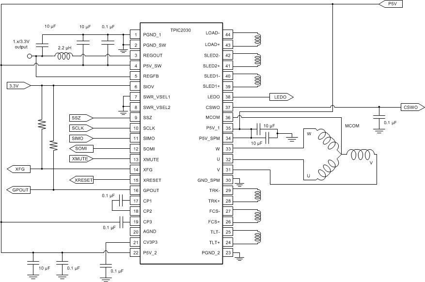 Figure 59. Example of Application Circuit
Table 39. Pin Connection When Specific Function is not Applied
| FUNCTION | PIN | NUMBER | CONNECTION |
|---|---|---|---|
| DC-DC converter | SWR_VSEL1 | 7 | GND |
| SWR_VSEL2 | 8 | GND | |
| P5V_SW | 4 | P5V | |
| PGND_SW | 2 | GND | |
| REGOUT | 3 | Open | |
| REGFB | 5 | P5V |
9.2.1 Design Requirements
To begin the design process, determine the following:
- Motor configuration: The user can use all motor channels or some of them.
- Power up devices with a 5-V supply.
9.2.2 Detailed Design Procedure
After power up on 5-V supply, the following values may be written to the following registers to enable motors.
- Set WRITE_ENABLE = 1 on REG76 via SPI.
- Set XSLEEP = 1 at REG70
- Enable motor channel by ENA_XXX bits on REG70
- Change the DAC settings for each motor in REG01-0B. Then, output channels will start driving load.
Table 40. Recommended External Components
| PIN | TO | FUNCTION | VALUE (rate) | UNIT |
|---|---|---|---|---|
| P5V_1 | PGND | Noise decoupling | 10.0 (10%16 V) | µF |
| P5V_2 | PGND | Noise decoupling | 10.0 (10%16 V) | µF |
| P5V_SW | PGND_SW | Noise decoupling | 10.0 (10%16 V) | µF |
| P5V_SPM | PGND | Noise decoupling | 10.0 (10%16 V) | µF |
| SIOV | PGND | Noise decoupling | 1.0 (10%10 V) | µF |
| REGOUT | REGFB | Inductor (ESR = 0.1 Ω) for DC-DC converter | 2.2 (20% 1.2 A) | µH |
| REGFB | PGND_SW | Capacitor (ESR = 0.025 Ω) | 10.0 (10%10 V) | µF |
| LOAD_P | PGND | Prevent surge current | 10000 (10% 16 V) | pF |
| LOAD_N | PGND | Prevent surge current | 10000(10% 16 V) | pF |
| CP1 | CP2 | Charge pump capacitor | 0.1 (10% 16 V) | µF |
| CP3 | P5V | Charge pump capacitor (P5V only, prohibit other power supply) | 0.1 (10% 16 V) | µF |
Table 41. Specific for DCDC Converter Components
| COMPONENTS | RECOMMENDED VALUE | RECOMMENDED SUPPLIER | PART NUMBER |
|---|---|---|---|
| Inductor | 2.2 (µH) | TAIYO YUDEN | BRL2518T2R2M |
| Capacitor | 10 (µF) | MURATA | GRM21BB31A106KE18L |
9.2.3 Application Curves
