SLIS110C April 2003 – March 2015 TPIC8101
PRODUCTION DATA.
- 1 Features
- 2 Applications
- 3 Description
- 4 Revision History
- 5 Description (continued)
- 6 Pin Configuration and Functions
- 7 Specifications
-
8 Detailed Description
- 8.1 Overview
- 8.2 Functional Block Diagram
- 8.3
Feature Description
- 8.3.1
Functional Terminal Description
- 8.3.1.1 Supply Voltage (VDD)
- 8.3.1.2 Ground (GND)
- 8.3.1.3 Reference Supply (Vref)
- 8.3.1.4 Buffered Integrator Output (OUT)
- 8.3.1.5 Integration/Hold Mode Selection (INT/HOLD)
- 8.3.1.6 Chip Select for SPI (CS)
- 8.3.1.7 Oscillator Input (XIN)
- 8.3.1.8 Oscillator Output (XOUT)
- 8.3.1.9 Data Output (SDO)
- 8.3.1.10 Data Input (SDI)
- 8.3.1.11 Serial Clock (SCLK)
- 8.3.1.12 Test (TEST)
- 8.3.1.13 Feedback Output for Amplifiers (CH1FB and CH2FB)
- 8.3.1.14 Input Amplifiers (CH1P, CH1N, CH2P, and CH2N)
- 8.3.2 Timing Information
- 8.3.1
Functional Terminal Description
- 8.4 Device Functional Modes
- 8.5 Programming
- 9 Application and Implementation
- 10Power Supply Recommendations
- 11Layout
- 12Device and Documentation Support
- 13Mechanical, Packaging, and Orderable Information
Package Options
Mechanical Data (Package|Pins)
- DW|20
Thermal pad, mechanical data (Package|Pins)
Orderable Information
1 Features
- Qualified for Automotive Applications
- AEC-Q100 Qualified With the Following Results:
- Device Temperature Grade 1: –40°C to 125°C Ambient Operating Temperature Range
- Device HBM Classification Level 3A
- Device CDM Classification Level C6
- Dual-Channel Knock Sensor Interface
- Programmable Input Frequency Prescaler (OSCIN)
- Serial Interface With Microprocessor (SPI)
- Programmable Gain
- Programmable Band-Pass Filter Center Frequency
- External Clock Frequencies up to 24 MHz
- 4, 5, 6, 8, 10, 12, 16, 20, and 24 MHz
- Programmable Integrator Time Constants
- Operating Temperature Range −40°C to 125°C
2 Applications
- Engine Knock Detector Signal Processing
- Analog Signal Processing With Filter Characteristics
3 Description
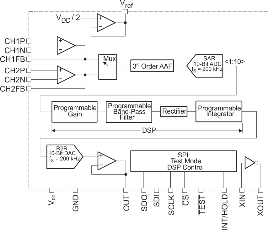
The TPIC8101 is a dual-channel signal processing IC for detection of premature detonation in combustion engine. The two sensor channels are selectable through the SPI bus. The knock sensor typically provides an electrical signal to the amplifier inputs. The sensed signal is processed through a programmable band-pass filter to extract the frequency of interest (engine knock or ping signals). The band-pass filter eliminates any engine background noise associated with combustion. The engine background noise is typically low in amplitude compared to the predetonation noise.
The detected signal is full-wave rectified and integrated by use of the INT/HOLD signal. The digital output from the integration stage is either converted to an analog signal, passed through an output buffer, or be read directly by the SPI.
This analog buffered output may be interfaced to an A/D converter and read by the microprocessor. The digital output may be directly interfaced to the microprocessor.
Device Information(1)
| PART NUMBER | PACKAGE | BODY SIZE (NOM) |
|---|---|---|
| TPIC8101 | SOIC (20) | 7.50 mm × 12.80 mm |
- For all available packages, see the orderable addendum at the end of the data sheet.
Simplified Schematic
