SLIS110C April 2003 – March 2015 TPIC8101
PRODUCTION DATA.
- 1 Features
- 2 Applications
- 3 Description
- 4 Revision History
- 5 Description (continued)
- 6 Pin Configuration and Functions
- 7 Specifications
-
8 Detailed Description
- 8.1 Overview
- 8.2 Functional Block Diagram
- 8.3
Feature Description
- 8.3.1
Functional Terminal Description
- 8.3.1.1 Supply Voltage (VDD)
- 8.3.1.2 Ground (GND)
- 8.3.1.3 Reference Supply (Vref)
- 8.3.1.4 Buffered Integrator Output (OUT)
- 8.3.1.5 Integration/Hold Mode Selection (INT/HOLD)
- 8.3.1.6 Chip Select for SPI (CS)
- 8.3.1.7 Oscillator Input (XIN)
- 8.3.1.8 Oscillator Output (XOUT)
- 8.3.1.9 Data Output (SDO)
- 8.3.1.10 Data Input (SDI)
- 8.3.1.11 Serial Clock (SCLK)
- 8.3.1.12 Test (TEST)
- 8.3.1.13 Feedback Output for Amplifiers (CH1FB and CH2FB)
- 8.3.1.14 Input Amplifiers (CH1P, CH1N, CH2P, and CH2N)
- 8.3.2 Timing Information
- 8.3.1
Functional Terminal Description
- 8.4 Device Functional Modes
- 8.5 Programming
- 9 Application and Implementation
- 10Power Supply Recommendations
- 11Layout
- 12Device and Documentation Support
- 13Mechanical, Packaging, and Orderable Information
Package Options
Mechanical Data (Package|Pins)
- DW|20
Thermal pad, mechanical data (Package|Pins)
Orderable Information
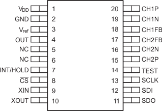
6 Pin Configuration and Functions
SOIC Package
(Top View)

Pin Functions
| PIN | TYPE (PULLUP/PULLDOWN) |
DESCRIPTION | |
|---|---|---|---|
| NAME | NO. | ||
| VDD | 1 | I | 5-V input supply |
| GND | 2 | I | Ground connection |
| Vref | 3 | O | Supply reference generator with external bypass capacitor |
| OUT | 4 | O | Buffered integrator output |
| NC(1) | 5 | — | No connection |
| 6 | |||
| INT/HOLD | 7 | I (pulldown) | Selectable for integrate (high) or hold (low) mode (with internal pulldown) |
| CS | 8 | I (pullup) | Chip select for SPI communications (active low with internal pullup) |
| XIN | 9 | I | Inverter input for oscillator |
| XOUT | 10 | O | Inverter output for oscillator |
| SDO | 11 | O | Serial data output for SPI bus |
| SDI | 12 | I (pullup) | Serial data input line |
| SCLK | 13 | I (pullup) | SPI clock |
| TEST | 14 | I (pullup) | Test mode (active low), open for normal operation |
| CH2P | 15 | I | Positive input for amplifier 2 |
| CH2N | 16 | I | Negative input for amplifier 2 |
| CH2FB | 17 | O | Output of amplifier 2, for feedback connection |
| CH1FB | 18 | O | Output of amplifier 1, for feedback connection |
| CH1N | 19 | I | Negative input for amplifier 1 |
| CH1P | 20 | I | Positive input for amplifier 1 |
(1) These terminals are to be used for test purposes only and are not connected in the system application. No signal traces should be connected to the NC terminals.