SLIS110C April 2003 – March 2015 TPIC8101
PRODUCTION DATA.
- 1 Features
- 2 Applications
- 3 Description
- 4 Revision History
- 5 Description (continued)
- 6 Pin Configuration and Functions
- 7 Specifications
-
8 Detailed Description
- 8.1 Overview
- 8.2 Functional Block Diagram
- 8.3
Feature Description
- 8.3.1
Functional Terminal Description
- 8.3.1.1 Supply Voltage (VDD)
- 8.3.1.2 Ground (GND)
- 8.3.1.3 Reference Supply (Vref)
- 8.3.1.4 Buffered Integrator Output (OUT)
- 8.3.1.5 Integration/Hold Mode Selection (INT/HOLD)
- 8.3.1.6 Chip Select for SPI (CS)
- 8.3.1.7 Oscillator Input (XIN)
- 8.3.1.8 Oscillator Output (XOUT)
- 8.3.1.9 Data Output (SDO)
- 8.3.1.10 Data Input (SDI)
- 8.3.1.11 Serial Clock (SCLK)
- 8.3.1.12 Test (TEST)
- 8.3.1.13 Feedback Output for Amplifiers (CH1FB and CH2FB)
- 8.3.1.14 Input Amplifiers (CH1P, CH1N, CH2P, and CH2N)
- 8.3.2 Timing Information
- 8.3.1
Functional Terminal Description
- 8.4 Device Functional Modes
- 8.5 Programming
- 9 Application and Implementation
- 10Power Supply Recommendations
- 11Layout
- 12Device and Documentation Support
- 13Mechanical, Packaging, and Orderable Information
Package Options
Mechanical Data (Package|Pins)
- DW|20
Thermal pad, mechanical data (Package|Pins)
Orderable Information
9 Application and Implementation
NOTE
Information in the following applications sections is not part of the TI component specification, and TI does not warrant its accuracy or completeness. TI’s customers are responsible for determining suitability of components for their purposes. Customers should validate and test their design implementation to confirm system functionality.
9.1 Application Information
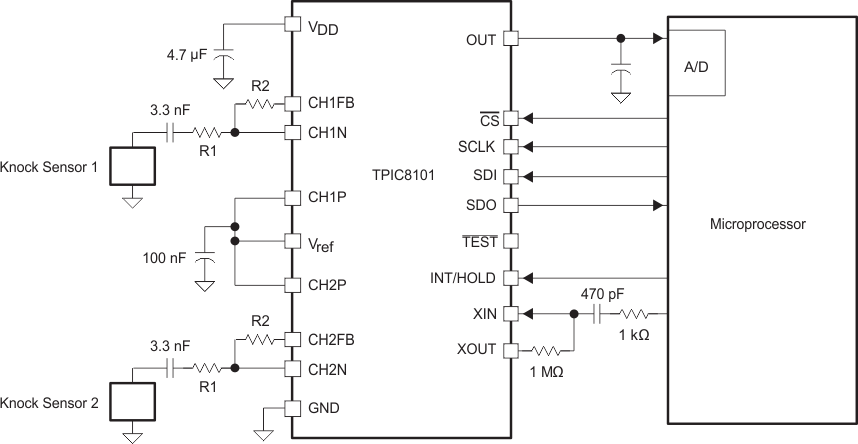
The TPIC8101 can interface with one or two flat type or resonant knock sense elements. Flat type (non-resonant) sensors have a wider frequency bandwidth than resonant type sensors. A microprocessor must also interface with the TPIC8101 as shown in Figure 5. The microprocessor may sample the output data either through SPI or by sampling the analog OUT signal.
9.2 Typical Application
 Figure 5. Application Schematic
9.2.1 Design Requirements
After the knock sense element and the microprocessor are chosen, the designer can choose the TPIC8101 settings. The settings that must be programmed through SPI are: ƒbp, ƒosc, AP, τC, and channel. If the analog output is used, then the INT/HOLD signal must be supplied by the microprocessor.
The input amplifier gain (AIN) is typically set to 1 by setting R1 = R2. R1 and R2 should be chosen to be greater than 25 kΩ.
Table 5. System Design Constraints
| PARAMETER | CONSTRAINT | VALUE FOR DESIGN EXAMPLE |
|---|---|---|
| VIN | Amplitude of input signal from knock sensor; determined by knock sensor specification | 300 mVpp |
| ƒbp | Bandpass center frequency; determined by knock sensor specification | 7.3 kHz |
| ƒosc | Oscillator frequency; determined by microprocessor | 6 MHz |
| tINT | Integration window; determined by system specification. This is half the period of the INT/HOLD signal (when using a 50% duty cycle) which is generated by the microprocessor. | 3 ms |
| VOUT | Maximum voltage on the OUT pin for the maximum VIN | 4.5 V |
9.2.2 Detailed Design Procedure
Design parameters to set:
AIN: Input amplifier gain, typically set to 1
AP: Programmable gain
τC: Integration time constant
Design equations:


Use Equation 2 to solve for AP:

For this design example, use the parameters specified in Table 5. This example is for a resonant knock sensor.
Using Equation 4:

Using Equation 5:

AP = 0.38
Table 6 lists the parameters to program.
Table 6. Parameters to Program
| Parameter | Calculated Value | Programmed Value | Code | SPI | |
|---|---|---|---|---|---|
| DEC | HEX | ||||
| Oscillator | 6 MHz | 6 MHz | 1000010 | ||
| Channel | 1 | 1 | 11100000 | ||
| ƒC0 | 7.3 kHz | 7.27 kHz | 42 | 2A | 101010 |
| AP | 0.38 | 0.381 | 34 | 22 | 10100010 |
| τC | 106 µs | 100 µs | 10 | 0A | 10001010 |
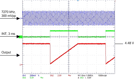
Figure 6 shows the input and output signals for this design example.
For a resonant knock sensor (as in the design example), the center frequency of the bandpass filter is set to the resonant frequency of the knock sensor. For a flat-type knock sensor, the bandpass filter design equation can be used to determine where the center frequency should be set.
The transfer function of the biquadratic bandpass IIR filter is:


9.2.3 Application Curve
 Figure 6. TPIC8101 Waveform