SLIS136C September   2011  – September 2019 TPL0501-100

PRODUCTION DATA.  

  1. Features
  2. Applications
  3. Description
    1.     Device Images
      1.      Simplified Schematic
  4. Revision History
  5. Pin Configuration and Functions
    1.     Pin Functions
  6. Specifications
    1. 6.1 Absolute Maximum Ratings
    2. 6.2 ESD Ratings
    3. 6.3 Thermal Information
    4. 6.4 Electrical Characteristics: Analog Specifications
    5. 6.5 Electrical Characteristics: Operating Specifications
    6. 6.6 Timing Requirements
    7. 6.7 Typical Characteristics
  7. Detailed Description
    1. 7.1 Overview
    2. 7.2 Functional Block Diagram
    3. 7.3 Feature Description
      1. 7.3.1 Single-Channel, 256-Position Resolution
    4. 7.4 Device Functional Modes
      1. 7.4.1 Voltage Divider Mode
      2. 7.4.2 Rheostat Mode
    5. 7.5 Programming
      1. 7.5.1 SPI Digital Interface
        1. Table 1. Register Map - Default Value 0x80
      2. 7.5.2 Ideal Resistance Values
  8. Application and Implementation
    1. 8.1 Application Information
    2. 8.2 Typical Application
      1. 8.2.1 Design Requirements
      2. 8.2.2 Detailed Design Procedure
      3. 8.2.3 Application Curve
  9. Power Supply Recommendations
    1. 9.1 Power Sequence
    2. 9.2 Wiper Position Upon Power Up
  10. 10Layout
    1. 10.1 Layout Guidelines
    2. 10.2 Layout Example
  11. 11Device and Documentation Support
    1. 11.1 Receiving Notification of Documentation Updates
    2. 11.2 Support Resources
    3. 11.3 Trademarks
    4. 11.4 Electrostatic Discharge Caution
    5. 11.5 Glossary
  12. 12Mechanical, Packaging, and Orderable Information

Package Options

Mechanical Data (Package|Pins)
Thermal pad, mechanical data (Package|Pins)
Orderable Information

Voltage Divider Mode

The digital potentiometer generates a voltage divider when all three terminals are used. The voltage divider at wiper-to-H and wiper-to-L is proportional to the input voltage at H to L (see Figure 12).
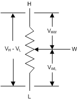
TPL0501-100 dfm_vt_mode_slis134.gifFigure 12. Equivalent Circuit for Voltage Divider Mode

For example, connecting terminal H to 5 V and terminal L to ground, the output voltage at terminal W can range from 0 V to 5 V (see Equation 1).

Equation 1. TPL0501-100 eq1_slis134.gif

The voltage difference between terminal H and terminal W can also be calculated in Equation 2.

Equation 2. TPL0501-100 eq2_slis134.gif

where

  • D is the decimal value of the wiper code.