SLIS136C September   2011  – September 2019 TPL0501-100

PRODUCTION DATA.  

  1. Features
  2. Applications
  3. Description
    1.     Device Images
      1.      Simplified Schematic
  4. Revision History
  5. Pin Configuration and Functions
    1.     Pin Functions
  6. Specifications
    1. 6.1 Absolute Maximum Ratings
    2. 6.2 ESD Ratings
    3. 6.3 Thermal Information
    4. 6.4 Electrical Characteristics: Analog Specifications
    5. 6.5 Electrical Characteristics: Operating Specifications
    6. 6.6 Timing Requirements
    7. 6.7 Typical Characteristics
  7. Detailed Description
    1. 7.1 Overview
    2. 7.2 Functional Block Diagram
    3. 7.3 Feature Description
      1. 7.3.1 Single-Channel, 256-Position Resolution
    4. 7.4 Device Functional Modes
      1. 7.4.1 Voltage Divider Mode
      2. 7.4.2 Rheostat Mode
    5. 7.5 Programming
      1. 7.5.1 SPI Digital Interface
        1. Table 1. Register Map - Default Value 0x80
      2. 7.5.2 Ideal Resistance Values
  8. Application and Implementation
    1. 8.1 Application Information
    2. 8.2 Typical Application
      1. 8.2.1 Design Requirements
      2. 8.2.2 Detailed Design Procedure
      3. 8.2.3 Application Curve
  9. Power Supply Recommendations
    1. 9.1 Power Sequence
    2. 9.2 Wiper Position Upon Power Up
  10. 10Layout
    1. 10.1 Layout Guidelines
    2. 10.2 Layout Example
  11. 11Device and Documentation Support
    1. 11.1 Receiving Notification of Documentation Updates
    2. 11.2 Support Resources
    3. 11.3 Trademarks
    4. 11.4 Electrostatic Discharge Caution
    5. 11.5 Glossary
  12. 12Mechanical, Packaging, and Orderable Information

Package Options

Mechanical Data (Package|Pins)
Thermal pad, mechanical data (Package|Pins)
Orderable Information

Application Curve

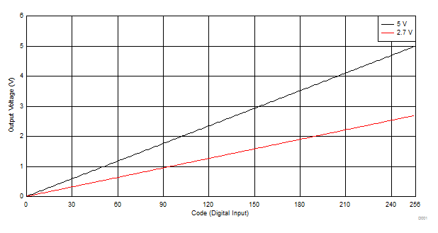
The voltage at terminal H determines the maximum analog voltage at the output. As the TPL0501 moves from zero-scale to full-scale, the voltage divider adjusts with relation to the voltage divider formula (see Figure 12), resulting in the desired voltage at terminal W. The voltage at terminal W ranges linearly from 0 V to the terminal H voltage. In this example, VIN at terminal H is 5 V and 2.7 V.
TPL0501-100 D001_SLIS135.gifFigure 19. TPL0501 Digital Input vs OPA320 Analog Output (DAC)