SLVSFI1A July 2021 – December 2021 TPS1HC100-Q1
PRODUCTION DATA
- 1 Features
- 2 Applications
- 3 Description
- 4 Revision History
- 5 Pin Configuration and Functions
- 6 Specifications
- 7 Parameter Measurement Information
-
8 Detailed Description
- 8.1 Overview
- 8.2 Functional Block Diagram
- 8.3
Feature Description
- 8.3.1 Accurate Current Sense
- 8.3.2 Programmable Current Limit
- 8.3.3 Inductive-Load Switching-Off Clamp
- 8.3.4
Full Protections and Diagnostics
- 8.3.4.1 Short-Circuit and Overload Protection
- 8.3.4.2 Open-Load and Short-to-Battery Detection
- 8.3.4.3 Short-to-Battery Detection
- 8.3.4.4 Reverse-Polarity and Battery Protection
- 8.3.4.5 Latch-Off Mode
- 8.3.4.6 Thermal Protection Behavior
- 8.3.4.7 UVLO Protection
- 8.3.4.8 Loss of GND Protection
- 8.3.4.9 Loss of Power Supply Protection
- 8.3.4.10 Reverse Current Protection
- 8.3.4.11 Protection for MCU I/Os
- 8.3.5 Diagnostic Enable Function
- 8.4 Device Functional Modes
- 9 Application and Implementation
- 10Power Supply Recommendations
- 11Layout
- 12Device and Documentation Support
- 13Mechanical, Packaging, and Orderable Information
Package Options
Mechanical Data (Package|Pins)
- PWP|14
Thermal pad, mechanical data (Package|Pins)
- PWP|14
Orderable Information
3 Description
The TPS1HC100-Q1 device is a fully protected high-side power switch, with integrated NMOS power FET and charge pump, targeted for the intelligent control of various loads. Accurate current sense and programmable current limit features differentiate it from the market.
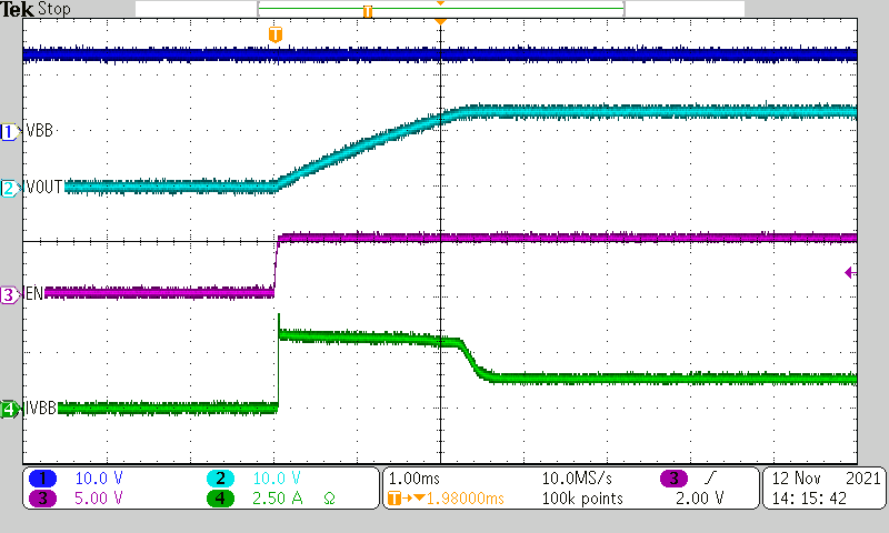
Low logic high threshold, VIH, of 1.5 V on the input pins allow use of MCUs GPIO signals to 1.8 V. High-accuracy current sensing provides a better real-time monitoring effect and more accurate diagnostics without further calibration. The external high-accuracy current limit allows setting the current limit value by application. The device highly improves the reliability of the system by effectively clamping the inrush current under start-up or short-circuit conditions. The TPS1HC100-Q1 device can be used as a high-side power switch for a wide variety of resistive, inductive, and capacitive loads, including low-wattage bulbs, LEDs, relays, solenoids, and heaters.
| PART NUMBER | PACKAGE | BODY SIZE (NOM) |
|---|---|---|
| TPS1HC100-Q1 | HTSSOP (14) | 4.40 mm × 5.00 mm |
 Capacitive Charging
Application