SLVSA01C May 2011 – June 2016 TPS2062-Q1 , TPS2065-Q1
PRODUCTION DATA.
- 1 Features
- 2 Applications
- 3 Description
- 4 Revision History
- 5 Pin Configuration and Functions
- 6 Specifications
- 7 Parameter Measurement Information
- 8 Detailed Description
-
9 Application and Implementation
- 9.1
Application Information
- 9.1.1 Overcurrent
- 9.1.2 OC Response
- 9.1.3 Undervoltage Lockout (UVLO)
- 9.1.4 Universal Serial Bus (USB) Applications
- 9.1.5 Host, Self-Powered (SPH), and Bus-Powered Hubs (BPH)
- 9.1.6 Low-Power Bus-Powered and High-Power Bus-Powered Functions
- 9.1.7 USB Power-Distribution Requirements
- 9.1.8 Generic Hot-Plug Applications
- 9.2 Typical Application
- 9.1
Application Information
- 10Power Supply Recommendations
- 11Layout
- 12Device and Documentation Support
- 13Mechanical, Packaging, and Orderable Information
Package Options
Mechanical Data (Package|Pins)
- DGN|8
Thermal pad, mechanical data (Package|Pins)
- DGN|8
Orderable Information
9 Application and Implementation
NOTE
Information in the following applications sections is not part of the TI component specification, and TI does not warrant its accuracy or completeness. TI’s customers are responsible for determining suitability of components for their purposes. Customers should validate and test their design implementation to confirm system functionality.
9.1 Application Information
9.1.1 Overcurrent
A sense FET is employed to check for overcurrent conditions. Unlike current-sense resistors, sense FETs do not increase the series resistance of the current path. When an overcurrent condition is detected, the device maintains a constant output current and reduces the output voltage accordingly. Complete shutdown occurs only if the fault is present long enough to activate thermal limiting.
Three possible overload conditions can occur. In the first condition, the output has been shorted before the device is enabled or before VI(IN) has been applied (see Figure 5). The TPS206x-Q1 senses the short and immediately switches into a constant-current output.
In the second condition, a short or an overload occurs while the device is enabled. At the instant the overload occurs, high currents may flow for a short period of time before the current-limit circuit can react. After the current-limit circuit has tripped (reached the overcurrent trip threshold), the device switches into constant-current mode.
In the third condition, the load has been gradually increased beyond the recommended operating current. The current is permitted to rise until the current-limit threshold is reached or until the thermal limit of the device is exceeded (see Figure 7). The TPS2065-Q1 and TPS2062-Q1 are capable of delivering current up to the current-limit threshold without damaging the device. Once the threshold has been reached, the device switches into its constant-current mode.
9.1.2 OC Response
The OCx open-drain output is asserted (active low) when an overcurrent or overtemperature shutdown condition is encountered after a 10-ms deglitch timeout. The output remains asserted until the overcurrent or overtemperature condition is removed. Connecting a heavy capacitive load to an enabled device can cause a momentary overcurrent condition; however, no false reporting on OCx occurs due to the 10-ms deglitch circuit. The TPS2065-Q1 and TPS2062-Q1 are designed to eliminate false overcurrent reporting. The internal overcurrent deglitch eliminates the need for external components to remove unwanted pulses. OCx is not deglitched when the switch is turned off due to an overtemperature shutdown.
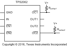 Figure 25. Typical Circuit for the OC Pin
9.1.3 Undervoltage Lockout (UVLO)
An undervoltage lockout ensures that the power switch is in the OFF state at power up. Whenever the input voltage falls below approximately 2 V, the power switch is quickly turned off. This facilitates the design of hot-insertion systems where it is not possible to turn off the power switch before input power is removed. The UVLO also keeps the switch from being turned ON until the power supply has reached at least 2 V, even if the switch is enabled. When the power supply returns, for example on cable reinsertion, the power switch is turned ON with a controlled rise time to reduce EMI and voltage overshoots.
9.1.4 Universal Serial Bus (USB) Applications
A typical application of the TPS206x-Q1 is for power distribution in USB applications. The universal serial bus (USB) interface is a 12-Mbps, or 1.5-Mbps, multiplexed serial bus designed for low-to-medium bandwidth PC peripherals (for example, keyboards, printers, scanners, and mice). The four-wire USB interface is conceived for dynamic attach-detach (hot plug-unplug) of peripherals. Two lines are provided for differential data, and two lines are provided for 5-V power distribution.
USB data is a 3.3-V level signal, but power is distributed at 5 V to allow for voltage drops in cases where power is distributed through more than one hub across long cables. Each function must provide its own regulated 3.3 V from the 5-V input or its own internal power supply.
The USB specification defines the following five classes of devices, each differentiated by power-consumption requirements:
- Hosts or self-powered hubs (SPH)
- Bus-powered hubs (BPH)
- Low-power, bus-powered functions
- High-power, bus-powered functions
- Self-powered functions
SPHs and BPHs distribute data and power to downstream functions. The TPS2065-Q1 and TPS2062-Q1 have higher current capability than required by one USB port; so, it can be used on the host side and supplies power to multiple downstream ports or functions.
NOTE
The USB interface and standards are continually being updated and expanded. Check the applicability of this product to the specific USB standard for which it is used.
9.1.5 Host, Self-Powered (SPH), and Bus-Powered Hubs (BPH)
Hosts and SPHs have a local power supply that powers the embedded functions and the downstream ports (see Figure 26). This power supply must provide from 5.25 V to 4.75 V to the board side of the downstream connection under full-load and no-load conditions. Hosts and SPHs are required to have current-limit protection and must report overcurrent conditions to the USB controller. Typical SPHs are desktop PCs, monitors, printers, and stand-alone hubs.
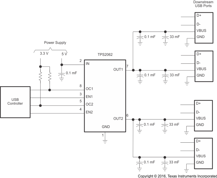 Figure 26. Typical Four-Port USB Host or Self-Powered Hub
BPHs obtain all power from upstream ports and often contain an embedded function. The hubs are required to power up with less than one unit load. The BPH usually has one embedded function, and power is always available to the controller of the hub. If the embedded function and hub require more than 100 mA on power up, the power to the embedded function may need to be kept off until enumeration is completed. This can be accomplished by removing power or by shutting off the clock to the embedded function. Power switching the embedded function is not necessary if the aggregate power draw for the function and controller is less than one unit load. The total current drawn by the bus-powered device is the sum of the current to the controller, the embedded function, and the downstream ports, and it is limited to 500 mA from an upstream port.
9.1.6 Low-Power Bus-Powered and High-Power Bus-Powered Functions
Both low-power and high-power bus-powered functions obtain all power from upstream ports; low-power functions always draw less than 100 mA; high-power functions must draw less than 100 mA at power up and can draw up to 500 mA after enumeration. If the load of the function is more than the parallel combination of 44 Ω and 10 μF at power up, the device must implement inrush current limiting (see Figure 27). With TPS2065-Q1 and TPS2062-Q1, the internal functions could draw more than 500 mA, which fits the needs of some applications such as motor driving circuits.
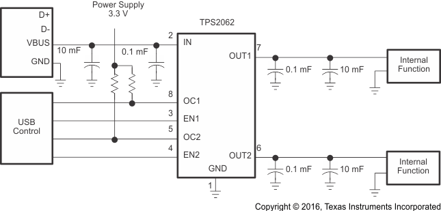 Figure 27. High-Power Bus-Powered Function
9.1.7 USB Power-Distribution Requirements
USB can be implemented in several ways, and, regardless of the type of USB device being developed, several power-distribution features must be implemented.
- Hosts or SPHs must:
- Current-limit downstream ports
- Report overcurrent conditions on USB VBUS
- BPHs must:
- Enable or disable power to downstream ports
- Power up at <100 mA
- Limit inrush current (<44 Ω and 10 μF)
- Functions must:
- Limit inrush currents
- Power up at <100 mA
The feature set of the TPS2065-Q1 and TPS2062-Q1 allows them to meet each of these requirements. The integrated current-limiting and overcurrent reporting is required by hosts and self-powered hubs. The logic-level enable and controlled rise times meet the need of both input and output ports on bus-powered hubs, as well as the input ports for bus-powered functions (see Figure 28).
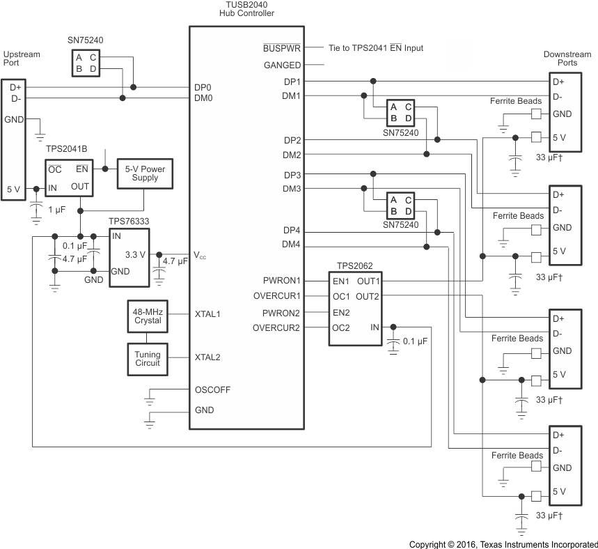 Figure 28. Hybrid Self- and Bus-Powered Hub Implementation
9.1.8 Generic Hot-Plug Applications
In many applications, it may be necessary to remove modules or PCBs while the main unit is still operating. These are considered hot-plug applications. Such implementations require the control of current surges seen by the main power supply and the card being inserted. The most effective way to control these surges is to limit and slowly ramp the current and voltage being applied to the card, similar to the way in which a power supply normally turns on. Due to the controlled rise times and fall times of the TPS2065-Q1 and TPS2062-Q1, these devices can be used to provide a softer start-up to devices being hot-plugged into a powered system. The UVLO feature of the TPS2065-Q1 and TPS2062-Q1 ensures that the switch is off after the card has been removed, and that the switch is off during the next insertion. The UVLO feature insures a soft start with a controlled rise time for every insertion of the card or module.
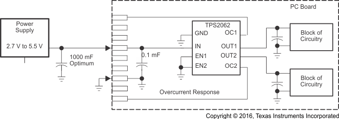 Figure 29. Typical Hot-Plug Implementation
By placing the TPS2065-Q1 and TPS2062-Q1 between the VCC input and the rest of the circuitry, the input power reaches these devices first after insertion. The typical rise time of the switch is approximately 1 ms, providing a slow voltage ramp at the output of the device. This implementation controls system surge currents and provides a hot-plugging mechanism for any device.
9.2 Typical Application
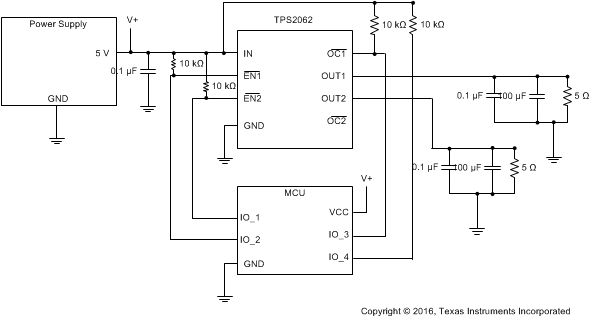 Figure 30. Typical Application Diagram
9.2.1 Design Requirements
The application requires distribution of 5 V to two seperate loads. The power supply can provide up to 4.5 A. In the case of a short circuit or overcurrent fault with a load, the supply to the other load must not be impacted. The load is equivalent to 5 Ω.
9.2.2 Detailed Design Procedure
The two channel current-limited switch, TPS2062-Q1 is used. Each switch provides a current limit maximum of 2.1 A from the 5-V supply in the case of a short circuit. Each channel is independently controlled through its ENx and has a corresponding OCx flag to alert the controller in the system of the overcurrent in the channel. This allows the other channel to independetly function in case of a short and the channel with the short to be disabled by the controller if the fault persists to ensure that the device does not have a thermal shut down. Take care to use proper thermal design of the PCB and application is made following the guidelines in Layout to help avoid potential thermal shut down.
A 0.1-μF capacitor was used as close as possible to IN to filter high frequencies on switching. A 0.1-μF capacitor was also used as close as possible to OUTx to filter high frequencies on switching and a 100-μF capacitor is used on each OUTx as bulk capacitance for each load. This application is shown in Figure 30.
9.2.3 Application Curves
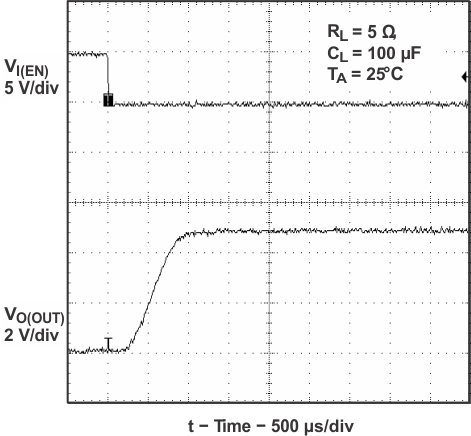
With 100 μF and 5-Ω Load
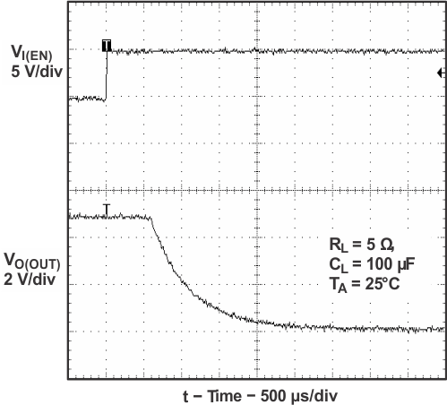
With 100 μF and 5-Ω Load