SLVSA01C May 2011 – June 2016 TPS2062-Q1 , TPS2065-Q1
PRODUCTION DATA.
- 1 Features
- 2 Applications
- 3 Description
- 4 Revision History
- 5 Pin Configuration and Functions
- 6 Specifications
- 7 Parameter Measurement Information
- 8 Detailed Description
-
9 Application and Implementation
- 9.1
Application Information
- 9.1.1 Overcurrent
- 9.1.2 OC Response
- 9.1.3 Undervoltage Lockout (UVLO)
- 9.1.4 Universal Serial Bus (USB) Applications
- 9.1.5 Host, Self-Powered (SPH), and Bus-Powered Hubs (BPH)
- 9.1.6 Low-Power Bus-Powered and High-Power Bus-Powered Functions
- 9.1.7 USB Power-Distribution Requirements
- 9.1.8 Generic Hot-Plug Applications
- 9.2 Typical Application
- 9.1
Application Information
- 10Power Supply Recommendations
- 11Layout
- 12Device and Documentation Support
- 13Mechanical, Packaging, and Orderable Information
Package Options
Mechanical Data (Package|Pins)
- DGN|8
Thermal pad, mechanical data (Package|Pins)
- DGN|8
Orderable Information
8 Detailed Description
8.1 Overview
The TPS206x-Q1 power-distribution switch is intended for applications where heavy capacitive loads and short circuits are likely to be encountered. This device incorporates 70-mΩ N-channel MOSFET power switches for power-distribution systems that require multiple power switches in a single package. Each switch is controlled by a logic enable input. Gate drive is provided by an internal charge pump designed to control the power-switch rise times and fall times to minimize current surges during switching. The charge pump requires no external components and allows operation from supplies as low as 2.7 V.
When the output load exceeds the current-limit threshold or a short is present, the device limits the output current to a safe level by switching into a constant-current mode, pulling the overcurrent (OCx) logic output low. When continuous heavy overloads and short circuits increase the power dissipation in the switch, causing the junction temperature to rise, a thermal protection circuit shuts off the switch to prevent damage. Recovery from a thermal shutdown is automatic once the device has cooled sufficiently (10°C hysteresis, typical). Internal circuitry ensures that the switch remains off until valid input voltage is present. This power-distribution switch is designed to set current limit at 1.5 A typically.
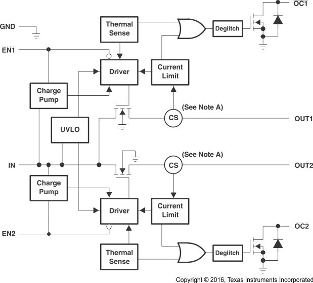
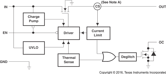
8.2 Functional Block Diagrams


8.3 Feature Description
8.3.1 Power Switch
The power switch is an N-channel MOSFET with a low ON-state resistance. Configured as a high-side switch, the power switch prevents current flow from OUT to IN and IN to OUT when disabled. The power switch supplies a minimum current of 1 A.
8.3.2 Charge Pump
An internal charge pump supplies power to the driver circuit and provides the necessary voltage to pull the gate of the MOSFET above the source. The charge pump operates from input voltages as low as 2.7 V and requires little supply current.
8.3.3 Driver
The driver controls the gate voltage of the power switch. To limit large current surges and reduce the associated electromagnetic interference (EMI) produced, the driver controls the rise and fall times of the output voltage.
8.3.4 Enable (ENx for TPS2062-Q1) and (EN for TPS2065-Q1)
The logic enable disables the power switch and the bias for the charge pump, driver, and other circuitry to reduce the supply current. The supply current is reduced to less than 1 μA when a logic high is present on ENx or a logic low is present on EN. A logic low input on ENx or logic high on EN restores bias to the drive and control circuits and turns the switch ON. The enable input is compatible with both TTL and CMOS logic levels.
8.3.5 Overcurrent (OCx)
The OCx open-drain output is asserted (active low) when an overcurrent or overtemperature condition is encountered. The output remains asserted until the overcurrent or overtemperature condition is removed. A 10‑ms deglitch circuit prevents the OCx signal from oscillation or false triggering. If an overtemperature shutdown occurs, the OCx is asserted instantaneously.
8.3.6 Current Sense
A sense FET monitors the current supplied to the load. The sense FET measures current more efficiently than conventional resistance methods. When an overload or short circuit is encountered, the current-sense circuitry sends a control signal to the driver. The driver in turn reduces the gate voltage and drives the power FET into its saturation region, which switches the output into a constant-current mode and holds the current constant while varying the voltage on the load.
8.3.7 Thermal Sense
The TPS2065-Q1 and TPS2062-Q1 implement a thermal sensing to monitor the operating temperature of the power distribution switch. In an overcurrent or short-circuit condition, the junction temperature rises. When the junction temperature rises to approximately 140°C, the internal thermal-sense circuitry turns off the switch, thus preventing the device from damage. Hysteresis is built into the thermal sense, and after the device has cooled approximately 10°C, the switch turns back ON. The switch continues to cycle OFF and ON until the fault is removed. The open-drain fault reporting output (OCx) is asserted (active low) when an overtemperature shutdown or overcurrent occurs.
8.3.8 Undervoltage Lockout
A voltage sense circuit monitors the input voltage. When the input voltage is below approximately 2 V, a control signal turns off the power switch.
8.4 Device Functional Modes
The device has two functional modes of operation controlled by EN or ENx. When there is a logic high on EN or a logic low on ENx, the device is in the normal mode of operation and the power switch is ON. When EN is logic low or ENx is logic high, the device is in a low power mode where the power switch is off and the supply current is reduced to less than 1 μA.