SLVSB97E July 2012 – January 2018 TPS23751 , TPS23752
PRODUCTION DATA.
- 1 Features
- 2 Applications
- 3 Description
- 4 Revision History
- 5 Pin Configuration and Functions
-
6 Specifications
- 6.1 Absolute Maximum Ratings
- 6.2 ESD Ratings
- 6.3 ESD Ratings: Surge
- 6.4 Recommended Operating Conditions
- 6.5 Thermal Information
- 6.6 Electric Characteristics - Controller Section
- 6.7 Electrical Characteristics - Sleep Mode (TPS23752 Only)
- 6.8 Electrical Characteristics - PoE Interface Section
- 6.9 Typical Characteristics
-
7 Detailed Description
- 7.1 Overview
- 7.2 Functional Block Diagrams
- 7.3 Feature Description
- 7.4
Device Functional Modes
- 7.4.1 PoE Overview
- 7.4.2
Sleep Mode Operation (TPS23752 only)
- 7.4.2.1 Converter Controller Features
- 7.4.2.2 PWM and VFO Operation; CTL, SRT, and SRD Pin Relationships to Output Load Current
- 7.4.2.3 Bootstrap Topology
- 7.4.2.4 Current Slope Compensation and Current Limit
- 7.4.2.5 RT
- 7.4.2.6 T2P, Startup and Power Management
- 7.4.2.7 Thermal Shutdown
- 7.4.2.8 Adapter ORing
- 7.4.2.9 Using DEN to Disable PoE
- 7.4.2.10 ORing Challenges
-
8 Application and Implementation
- 8.1 Application Information
- 8.2
Typical Application
- 8.2.1 Design Requirements
- 8.2.2
Detailed Design Procedure
- 8.2.2.1 Input Bridges and Schottky Diodes
- 8.2.2.2 Protection, D1
- 8.2.2.3 Capacitor, C1
- 8.2.2.4 Detection Resistor, RDEN
- 8.2.2.5 Classification Resistor, RCLS
- 8.2.2.6 APD Pin Divider Network, RAPD1, RAPD2
- 8.2.2.7 Setting the PWM-VFO Threshold using the SRT pin
- 8.2.2.8 Setting Frequency (RT)
- 8.2.2.9 Current Slope Compensation
- 8.2.2.10 Voltage Feed-Forward Compensation
- 8.2.2.11 Estimating Bias Supply Requirements and Cvc
- 8.2.2.12 Switching Transformer Considerations and RVC
- 8.2.2.13 T2P Pin Interface
- 8.2.2.14 Softstart
- 8.2.2.15 Special Switching MOSFET Considerations
- 8.2.2.16 ESD
- 8.2.2.17 Thermal Considerations and OTSD
- 8.2.3 Application Curves
- 9 Power Supply Recommendations
- 10Layout
- 11Device and Documentation Support
- 12Mechanical, Packaging, and Orderable Information
Package Options
Mechanical Data (Package|Pins)
- PWP|16
Thermal pad, mechanical data (Package|Pins)
- PWP|16
Orderable Information
5 Pin Configuration and Functions
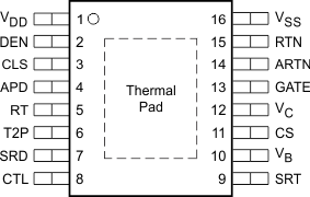
PWP Package
16-Pin TSSOP
Top View

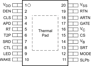
PWP Package
20-Pin TSSOP
Top View

Pin Functions
| NAME | PIN | I/O | DESCRIPTION | |
|---|---|---|---|---|
| TPS23751 | TPS23752 | |||
| VDD | 1 | 1 | I | Connect to positive PoE input power rail. Bypass with 0.1 µF to VSS. |
| DEN | 2 | 2 | I/O | Connect 24.9 kΩ to VDD for detection. Pull to VSS to disable pass MOSFET. |
| CLS | 3 | 3 | I/O | Connect resistor from CLS to VSS to program classification current. |
| APD | 4 | 4 | I | Raise 1.5 V above ARTN to disable pass MOSFET and force T2P active. |
| RT | 5 | 5 | I | Connect a resistor from RT to ARTN to set switching frequency. |
| T2P | 6 | 6 | O | Active low indicates type-2 PSE connected or APD active. |
| SRD | 7 | 7 | O | Disable external synchronous rectifiers in VFO Mode. |
| CTL | 8 | 8 | I | Control loop input to PWM |
| LED | — | 9 | O | Open-drain drive for external LED controlled by SLPb, MODE, and WAKE. |
| WAKE | — | 10 | I/O | Pull WAKE low to re-enable the DC-DC converter from Sleep Mode. |
| SLPb | — | 11 | I | Pull low during normal operation to enter Sleep Mode. |
| MODE | — | 12 | I | Enables pulsed MPS when entering Sleep Mode. Control LED in normal operation. |
| SRT | 9 | 13 | I | Set the threshold of PWM to VFO transition |
| VB | 10 | 14 | O | 5 V bias supply. Bypass with a minimum of 0.1 µF to ARTN. |
| CS | 11 | 15 | I/O | Current sense input. Connect to ARTN-referenced current sense resistor. |
| VC | 12 | 16 | I/O | DC-DC converter bias voltage. Bypass with 0.47 µF or more to ARTN directly at pin. |
| GATE | 13 | 17 | O | Gate driver output for DC-DC converter switching MOSFET. |
| ARTN | 14 | 18 | PWR | DC-DC converter analog return. Connect to RTN. |
| RTN | 15 | 19 | O | Drain of PoE pass MOSFET. Connect to ARTN. |
| VSS | 16 | 20 | PWR | Connect to negative power rail derived from PoE source. |
| Pad | — | Always connect PowerPAD™ to VSS. A large fill area is required to assist in heat dissipation. | ||