SLVS728D January 2007 – October 2019 TPS2412 , TPS2413
PRODUCTION DATA.
- 1 Features
- 2 Applications
- 3 Description
- 4 Revision History
- 5 Device Comparison Table
- 6 Pin Configuration and Functions
- 7 Specifications
-
8 Detailed Description
- 8.1 Overview
- 8.2 Functional Block Diagram
- 8.3
Feature Description
- 8.3.1 Definitions
- 8.3.2 TPS2412 vs TPS2413 – MOSFET Control Methods
- 8.3.3 N+1 Power Supply – Typical Connection
- 8.3.4 Input ORing – Typical Connection
- 8.3.5 System Design and Behavior With Transients
- 8.3.6 TPS2412 Regulation-Loop Stability
- 8.3.7 MOSFET Selection and R(RSET)
- 8.3.8 Gate Drive, Charge Pump and C(BYP)
- 8.4 Device Functional Modes
- 9 Application and Implementation
- 10Power Supply Recommendations
- 11Layout
- 12Device and Documentation Support
- 13Mechanical, Packaging, and Orderable Information
Package Options
Refer to the PDF data sheet for device specific package drawings
Mechanical Data (Package|Pins)
- D|8
- PW|8
Thermal pad, mechanical data (Package|Pins)
Orderable Information
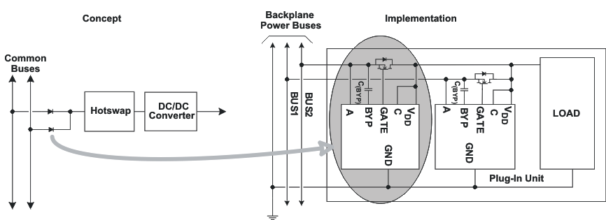
8.3.4 Input ORing – Typical Connection
Figure 10 shows how redundant buses may be ORed to a common point to achieve higher reliability. It is possible to have both MOSFETs ON at once if the bus voltages are matched, or the combination of tolerance and regulation causes both TPS2412/13 circuits to see a forward voltage. The ORing MOSFET disconnects the lower-voltage bus, protecting the remaining bus from potential overload by a fault.
 Figure 10. Example ORing of Input Power Buses