SLVS728D January   2007  – October 2019 TPS2412 , TPS2413

PRODUCTION DATA.  

  1. Features
  2. Applications
  3. Description
    1.     Device Images
      1.      Typical Application Diagram
  4. Revision History
  5. Device Comparison Table
  6. Pin Configuration and Functions
    1.     Pin Functions
  7. Specifications
    1. 7.1 Absolute Maximum Ratings
    2. 7.2 ESD Ratings
    3. 7.3 Recommended Operating Conditions
    4. 7.4 Thermal Information
    5. 7.5 Electrical Characteristics
    6. 7.6 Dissipation Ratings
    7. 7.7 Typical Characteristics
  8. Detailed Description
    1. 8.1 Overview
    2. 8.2 Functional Block Diagram
    3. 8.3 Feature Description
      1. 8.3.1 Definitions
      2. 8.3.2 TPS2412 vs TPS2413 – MOSFET Control Methods
      3. 8.3.3 N+1 Power Supply – Typical Connection
      4. 8.3.4 Input ORing – Typical Connection
      5. 8.3.5 System Design and Behavior With Transients
      6. 8.3.6 TPS2412 Regulation-Loop Stability
      7. 8.3.7 MOSFET Selection and R(RSET)
      8. 8.3.8 Gate Drive, Charge Pump and C(BYP)
    4. 8.4 Device Functional Modes
  9. Application and Implementation
    1. 9.1 Application Information
    2. 9.2 Typical Application
      1. 9.2.1 Design Requirements
      2. 9.2.2 Detailed Design Procedure
      3. 9.2.3 Application Curves
  10. 10Power Supply Recommendations
    1. 10.1 Recommended Operating Range
    2. 10.2 VDD, BYP, and Powering Options
  11. 11Layout
    1. 11.1 Layout Guidelines
    2. 11.2 Layout Example
  12. 12Device and Documentation Support
    1. 12.1 Related Links
    2. 12.2 Community Resources
    3. 12.3 Trademarks
    4. 12.4 Electrostatic Discharge Caution
    5. 12.5 Glossary
  13. 13Mechanical, Packaging, and Orderable Information

Package Options

Refer to the PDF data sheet for device specific package drawings

Mechanical Data (Package|Pins)
  • D|8
  • PW|8
Thermal pad, mechanical data (Package|Pins)
Orderable Information

Typical Characteristics

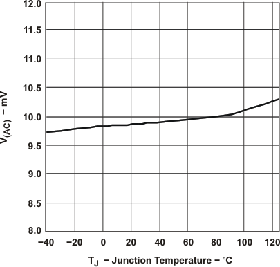
TPS2412 TPS2413 regv_v_tj_lvs728.gif
Figure 1. TPS2412 V(AC) Regulation Voltage vs Temperature
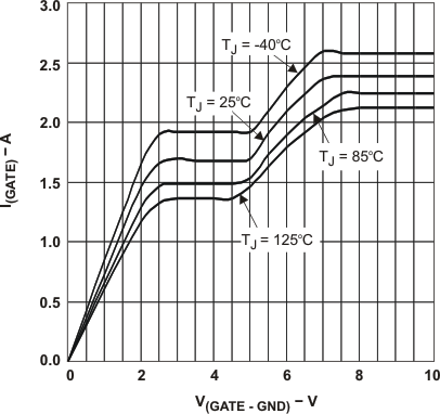
TPS2412 TPS2413 pulse_v_gatev_lvs728.gif
Figure 3. Pulsed Gate Sinking Current vs Gate Voltage
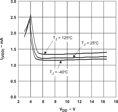
TPS2412 TPS2413 idd_v_vdd_lvs728.gif
Figure 5. VDD Current vs VDD Voltage (Gate Saturated High)
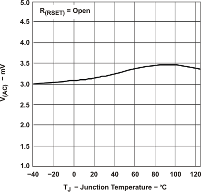
TPS2412 TPS2413 toff_v_tj_lvs728.gif
Figure 2. Fast Turnoff Threshold vs Temperature
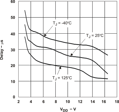
TPS2412 TPS2413 ton_v_vdd_lvs728.gif
Figure 4. Turnon Delay vs VDD (Power Applied Until Gate is Active)
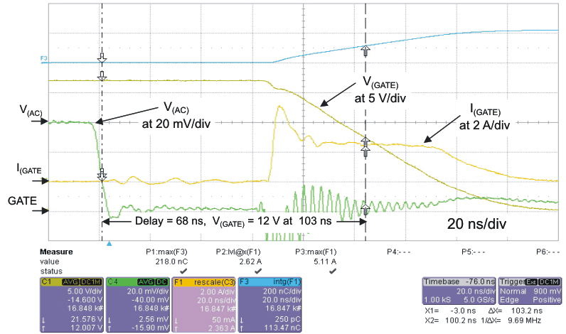
TPS2412 TPS2413 toff_10nf_12v_lvs728.gif
Figure 6. Turnoff Time With
C(GATE) = 10 nF and V(AC) = -20 mV (VDD = VA = 12 V)
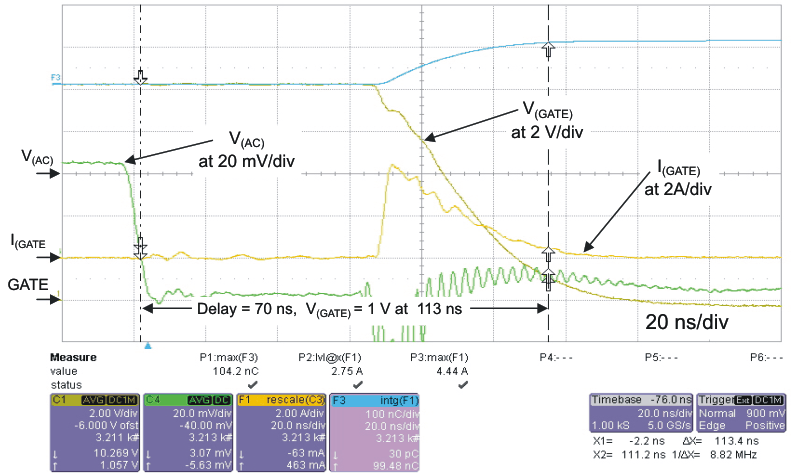
TPS2412 TPS2413 toff_10nf_1v_lvs728.gif
Figure 7. Turnoff Time With
C(GATE) = 10 nF and V(AC) = -20 mV (VDD = 5, VA = 1 V)