SPAS093C December 2009 – September 2015 TPS2505
PRODUCTION DATA.
- 1 Features
- 2 Applications
- 3 Description
- 4 Revision History
- 5 Pin Configuration and Functions
-
6 Specifications
- 6.1 Absolute Maximum Ratings
- 6.2 ESD Ratings
- 6.3 Recommended Operating Conditions
- 6.4 Thermal Information
- 6.5 Electrical Characteristics (Shared Boost, LDO and USB)
- 6.6 Electrical Characteristics (Boost Only)
- 6.7 Electrical Characteristics (USB1/2 Only)
- 6.8 Electrical Characteristics (LDO and Reset Only)
- 6.9 Recommended External Components
- 6.10 Dissipation Ratings
- 6.11 Typical Characteristics
- 7 Parameter Measurement Information
-
8 Detailed Description
- 8.1 Overview
- 8.2 Functional Block Diagram
- 8.3
Feature Description
- 8.3.1 PGND
- 8.3.2 IN
- 8.3.3 EN
- 8.3.4 GND
- 8.3.5 ILIM1/2
- 8.3.6 RESET
- 8.3.7 LDOOUT
- 8.3.8 LDOIN
- 8.3.9 ENLDO
- 8.3.10 FAULT1/2
- 8.3.11 ENUSB1/2
- 8.3.12 USB1/2
- 8.3.13 AUX
- 8.3.14 SW
- 8.3.15 Thermal Pad
- 8.3.16 Boost Converter
- 8.3.17 USB Switches
- 8.3.18 3.3-V LDO
- 8.3.19 Reset Comparator
- 8.3.20 Thermal Shutdown
- 8.3.21 Component Recommendations
- 8.4 Device Functional Modes
-
9 Application and Implementation
- 9.1 Application Information
- 9.2
Typical Application
- 9.2.1 Design Requirements
- 9.2.2 Detailed Design Procedure
- 9.2.3 Application Curves
- 10Power Supply Recommendations
- 11Layout
- 12Device and Documentation Support
- 13Mechanical, Packaging, and Orderable Information
Package Options
Mechanical Data (Package|Pins)
- RGW|20
Thermal pad, mechanical data (Package|Pins)
- RGW|20
Orderable Information
1 Features
- Integrated Synchronous Boost Converter, LDO, and Dual USB Current-Limited Switches
- 1.8-V to 5.25-V Input Voltage
(2.2-V Minimum Start-Up Voltage) - Adjustable Independent USB Current Limit
- 100 mA to 1100 mA
- Auxiliary 5.1-V Output
- 3.3-V Linear Regulator Output
- Inrush Current < 100 mA
- Minimal External Components Required
- Deglitched Independent Fault Reporting
- Small 5-mm × 5-mm QFN-20 Package
- Industrial Temperature Range
2 Applications
- Portable Applications Using Single Li+ Cell
- Bus Powered USB Hosts
- USB Hosts Without Native 5-V Supplies
- Computer Peripherals
3 Description
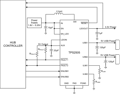
The TPS2505 device provides an integrated solution to meet USB 5-V power requirements from a 1.8-V to 5.25-V input supply. The features include a 5.1-V, 1100-mA boost converter, a 200-mA, 3.3-V LDO linear regulator and dual USB 2.0 compliant power outputs with independent output switch enable, current limit, and overcurrent fault reporting.
The 1.8-V to 5.25-V input can be supplied by sources including DC-DC regulated supplies (for example, 3.3 V), or batteries such as single cell Li+, two-cell or three-cell NiCd, NiMH or alkaline.
The output trip current for the dual USB switches can be programmed through external resistors from as low as 100 mA to as high as 1100 mA.
An auxiliary 5.1-V output is provided, where the total current supplied by the USB outputs and the auxiliary by cannot exceed 1100 mA.
Device Information(1)
| PART NUMBER | PACKAGE | BODY SIZE (NOM) |
|---|---|---|
| TPS2505 | VQFN (20) | 5.00 mm × 5.00 mm |
- For all available packages, see the orderable addendum at the end of the data sheet.
Typical Application
